Another Bootstrap for a ROM less system

Re: Another Bootstrap for a ROM less system
According to the datasheet two cycles should be enough and in my reset cycles I always create four cycles or more. So this should not be the problem.
Re: Another Bootstrap for a ROM less system
Just to give an update the proof of concept is done and works. I can now "IML" a ROM Image into my test setup via the AVR and then switch the 6502 to normal operation and start the monitor program. All the anomalies I have seen disappeared after I have replaced the GAL (the one I used first seems to be broken, at least some outputs never went above 2.5V) and corrected some wrong wires on my breadboard. Now the next step is to clean up the AVR code and write a decent documentation.
Re: Another Bootstrap for a ROM less system
Here an update with some documentation. First the schematic. I added an ACIA and two TIL311 hex displays to debug (single step through the data bus).
Next is the assembler source of the current version of the AVR monitor that controls the bootstrap process
And the Design file of the currently used GAL
To boot the 6502 system you need to connect a terminal to the USART of the AVR because at the moment the AVR monitor does nothing at bootstrap. You need to tell him what to do to bootstrap the 6502 system (that will change when the real version will be implemented)
First the AVR sends the mandatory greeting (Hello World) and then prompts for commands (*).
So that's all what is going to happen in that project. Things that are missing is a upload of new rom images via XMODEM and a default startup sequence, but this is not really difficult, so I will not test it in the POC. This will be integrated into my next SBC project. In other words I can say farewell ROMs, EPROMs, EEROMs et.al. and no more I will be concerned by the speed of ROMs.
Cheers
Peter
Next is the assembler source of the current version of the AVR monitor that controls the bootstrap process
And the Design file of the currently used GAL
Code: Select all
Name     avr-iml ;
PartNo   00 ;
Date     25.07.2015 ;
Revision 01 ;
Designer cbscpe ;
Company  privat ;
Assembly None ;
Location  ;
Device   g22v10 ;

/* *************** INPUT PINS *********************/
PIN    1 =  IML                    ; /*                                 */
PIN    2 =  A15                    ; /*                                 */
PIN    3 =  A14                    ; /*                                 */
PIN    4 =  A13                    ; /*                                 */
PIN    5 =  A12                    ; /*                                 */
PIN    6 =  A11                    ; /*                                 */
PIN    7 =  A10                    ; /*                                 */
PIN    8 =  A9                     ; /*                                 */
PIN    9 =  A8                     ; /*                                 */
PIN   10 =  A7                     ; /*                                 */
PIN   11 =  A6                     ; /*                                 */
PIN   13 =  RW                     ; /*                                 */
PIN   14 =  PHI2                   ; /*                                 */

/* *************** OUTPUT PINS *********************/
PIN   15 = !LE                     ; /*                                 */
PIN   16 = !IOB                    ; /*                                 */
PIN   17 = !IOC                    ; /*                                 */
PIN   18 = !RAM                    ; /*                                 */
PIN   19 = !BYTE                   ; /*                                 */
PIN   20 = !RD                     ; /*                                 */
PIN   21 = !WR                     ; /*                                 */


FIELD	ADDRESS = [A15..0];


RD	=  RW  &  PHI2;

WR	= !RW  &  PHI2;

LE	=  PHI2;

IOB	=  ADDRESS:[C040..C07F] & !IML;

IOC	=  ADDRESS:[C080..C0FF] & !IML
	#  ADDRESS:[C080..C0FF] &  IML  & !RW;

BYTE	=                          IML  &  RW  &  PHI2
	#  ADDRESS:[C000..C03F] & !IML  &  RW  &  PHI2;

RAM    =                         IML  & !RW
	# ADDRESS:[0000..BFFF] & !IML
	# ADDRESS:[C100..FFFF] & !IML  &  RW;
Code: Select all
Hello World

*y

*0k

*1ri?0r
PHI2:0, IML:0, RES:0

*
Code: Select all
y       Load the default ROM image via the IML process, this sends a loop of the three instructions LDA #imm, STA address, JMP LOOP until the ROM Image has been loaded
0k      Starts Timer 2 as PHI2. The value is the byte loaded into OCR2A, 0 means the fastests and PHI2 will be half the clock rate of the AVR, which uses a 22MHz clock. In other words the system is clocked with 11MHz and even I use a 70ns RAM and a 4MHz ACIA (CDP65C51) this works perfect, 64k gives a clock of about 100kHz, ffk gives a clock of about 40kHz
1r      Assert 6502 RESET line
i       Toggle (at that moment clear) the IML bit that is activate normal memory map (after the AVR is powered up it is set and the bootstrap mode is activated in the GAL, required by the y command) .
?       Show the status of PHI2, IML and RES, it is just used to make sure IML is cleared and give the 6502 some PHI2 pulses
0r      De-Assert 6502 RESET and start whatever has been loaded in the ROM
Cheers
Peter
-
jac_goudsmit

- Posts: 229
- Joined: 23 Jun 2011
- Location: Rancho Cucamonga, California
- Contact:
Re: Another Bootstrap for a ROM less system
BigEd wrote:
If you see something which sometimes happens and sometimes doesn't, I think probably you are not holding reset for long enough.
During the 6 clock cycles of the reset cycle you will see what looks like the 65C02 handling an interrupt (it accesses the stack in descending order) except R/~W is high the whole time.
===Jac

Re: Another Bootstrap for a ROM less system
The Datasheet for my Rockwell R65C02 says seven clock cycles which is what I saw in my experiments back in January 2014. Is the WDC 65C02 different?
-
jac_goudsmit
- Posts: 229
- Joined: 23 Jun 2011
- Location: Rancho Cucamonga, California
- Contact:
Re: Another Bootstrap for a ROM less system
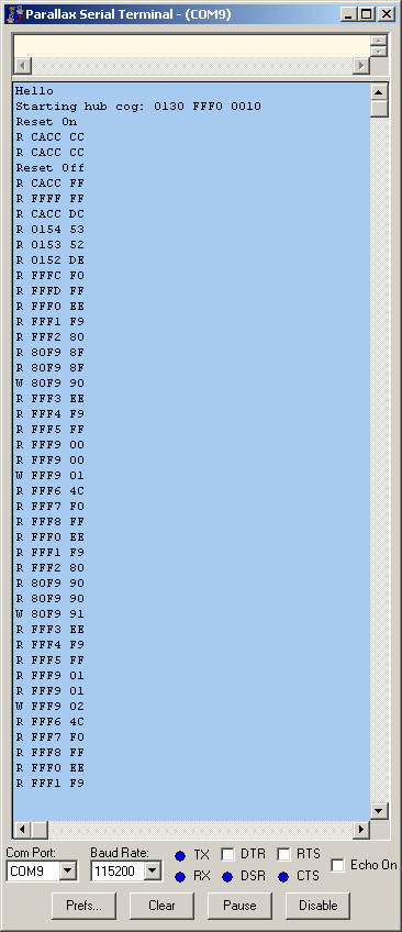
Here's a trace from my Propeddle project which uses the WDC65C02:
I pull RESET low and high while the CLK0 input is low. If you look carefully you'll see that a memory location ($CACC) appears to change without writing but that happened because there was no device at that location so the data is unreliable because the data bus wasn't being driven by anything. I had a small program in (pseudo) ROM that incremented a location and looped.
From your trace dump, it looks like my WDC65C02 uses one more cycle after RESET goes high before it gets the reset vector.
http://propeddle.com/wp-content/uploads ... .15.38.png
===Jac
Re: Another Bootstrap for a ROM less system
Hi Jac,
Section 3.11 in the W65C02S Datasheet states that the reset sequence takes seven cycles (same as the R65C02). I assume that includes the two cycles that read the reset vector from memory locations $FFFC and $FFFD.
I was toggling the reset line on my R65C02 while the Φ0 clock input was high. I wonder if that makes a difference in the cycle count?
Re: Another Bootstrap for a ROM less system
According to the W65C816 and W65C02S datasheets RES is sampled with the falling edge of PHI2. You need to respect tpch and tpcs (processor control hold and processor control setup time) In other words if you de-assert RES when PHI2 is high then you will see 5 cycles and then in cycle 6 and 7 the CPU will fetch the reset vector. When you de-assert RES when PHI2 is low you need an additional cycle for the CPU to sample RES at the falling edge. I could verify this with my setup.
Edit: I have to re-check, I'm not really sure this worked with my setup. Something is strange here.
Edit: I have to re-check, I'm not really sure this worked with my setup. Something is strange here.
Re: Another Bootstrap for a ROM less system
That could explain why Jac's description of the reset sequence is off by one cycle.
Re: Another Bootstrap for a ROM less system
It's rather that I observe the same as jac.
Reset is de-asserted with PHI2 = Low (w creates a short positive pulse on PHI2). You see the result "PHI2:0, IML:0, RES:1" of the ? command. The I toogle PHI2 (p command) and display that signals and the processor status with PHI2=high. Then I continuously toggle PHI2 twice (first p produces a high to low transition and the second p a low to high transition) and display always the signals and the processor status (VDA, VPA and VPB). And surprisingly it is the 7th cycle after the cycle that detects that reset was released which requests the vector (VPB low). And if I consult an old Synertek datasheet it says
So exactly what the output of jac Parallax and my IML logic says. So I'd say it is six cycles after the CPU detects reset is de-asserted before he fetches the program counter from reset vector locations.
Peter
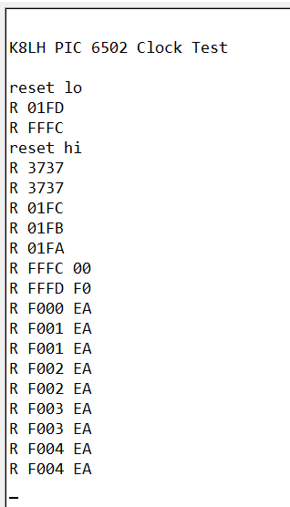
Code: Select all
*1rww0r?
PHI2:0, IML:0, RES:1

*ps?
VPA:0, VDA:0, VPB:0, R/W:1
PHI2:1, IML:0, RES:1

*pps?
VPA:0, VDA:0, VPB:0, R/W:1
PHI2:1, IML:0, RES:1

*pps?
VPA:1, VDA:1, VPB:1, R/W:1
PHI2:1, IML:0, RES:1

*pps?
VPA:0, VDA:0, VPB:1, R/W:1
PHI2:1, IML:0, RES:1

*pps?
VPA:0, VDA:1, VPB:1, R/W:1
PHI2:1, IML:0, RES:1

*pps?
VPA:0, VDA:1, VPB:1, R/W:1
PHI2:1, IML:0, RES:1

*pps?
VPA:0, VDA:1, VPB:1, R/W:1
PHI2:1, IML:0, RES:1

*pps?
VPA:0, VDA:1, VPB:0, R/W:1
PHI2:1, IML:0, RES:1

*Quote:
After a system initialization time of six clock cycles, the mask interrupt flag will be set and the microprocessor will load the program counter from memory locations FFFC and FFFD.
Peter
Re: Another Bootstrap for a ROM less system
Peter, how would someone explain the discrepancy from the WDC Datasheet?
Re: Another Bootstrap for a ROM less system
I don't know yet. I don't think it is because I statically step through the states, the W65C816 is supposed to be fully static. The strange thing is that the sequence of the cycles is not as described in Table 5-7 section 22a of the data sheet. And what is in the datasheet is not what the legacy 6502 was doing. In any case this is not a problem for the bootstrap solution described here as I have VPB connected to an input Pin of the AVR and just created cycles until VPB=Low. Now I know how many cycle my "real" W65C816 uses I can just create the number of cycles the CPU expects.
-
BigDumbDinosaur

- Posts: 9428
- Joined: 28 May 2009
- Location: Midwestern USA (JB Pritzker’s dystopia)
- Contact:
Re: Another Bootstrap for a ROM less system
cbscpe wrote:
I don't know yet. I don't think it is because I statically step through the states, the W65C816 is supposed to be fully static. The strange thing is that the sequence of the cycles is not as described in Table 5-7 section 22a of the data sheet. And what is in the datasheet is not what the legacy 6502 was doing. In any case this is not a problem for the bootstrap solution described here as I have VPB connected to an input Pin of the AVR and just created cycles until VPB=Low. Now I know how many cycle my "real" W65C816 uses I can just create the number of cycles the CPU expects.
x86? We ain't got no x86. We don't NEED no stinking x86!