6502.org Forum  Projects  Code  Documents  Tools  Forum
It is currently Sat Nov 23, 2024 2:42 am

All times are UTC


Post new topic Reply to topic  [ 842 posts ]  Go to page Previous  1 ... 3, 4, 5, 6, 7, 8, 9 ... 57  Next
Author Message
PostPosted: Sun Jul 12, 2015 7:59 pm 
Offline
User avatar

Joined: Mon May 25, 2015 2:25 pm
Posts: 690
Location: Gillies, Ontario, Canada
Finally a rainy Sunday afternoon!

Managed to get the AVR jacked in, and so far every part of the circuitry, including the GPU bus switch has passed the tests.
I wrote a simple program to take 24 bit bitmaps and convert them to RRR-GGG-BB format data for AVR GCC.
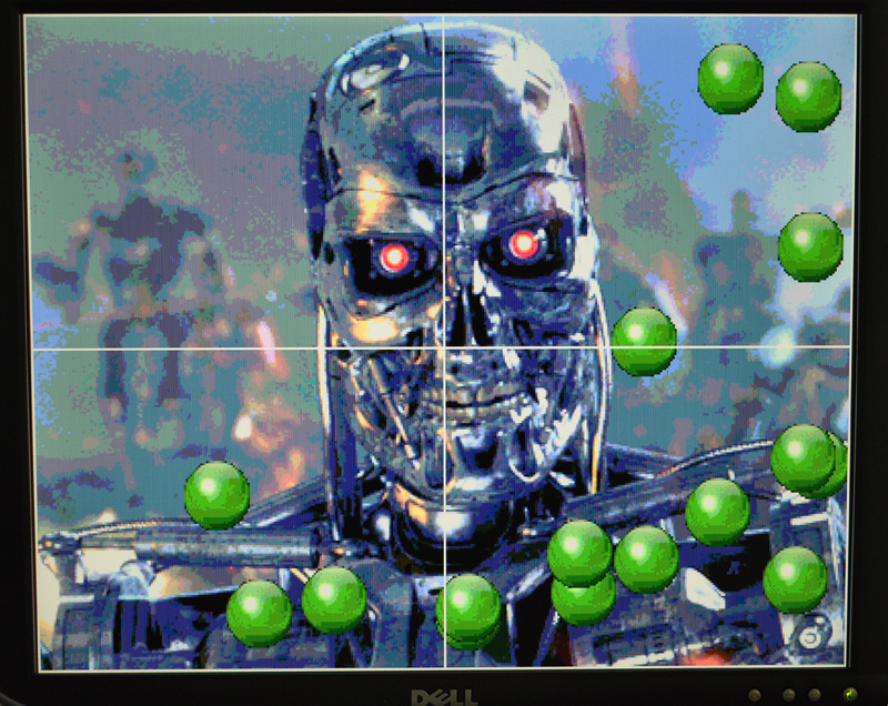
Loaded a 400x300 image into the AVR-1284, and then coded a border and some ball sprites to test the buffer switching.

Image
An AVR-1284 used for testing the system.

The AVR is only temporary, so the wiring is ugly!

Image
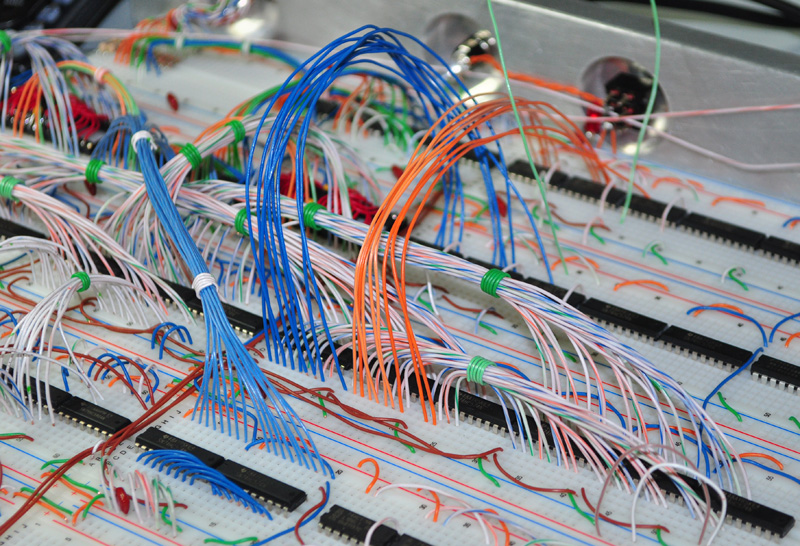
The AVR pretends to be a GPU, but is much slower.

Orange wires are address lines (18 buts), blue wires are data bus (8 bits).
AVR also listens to V-Sync (1 bit) and controls Video Memory buffer switching (1 bit).

The AVR can do maybe 1 million pixels per second at best.
The GPU will be 20 times faster, running purely at 20MHz.
Funny, the AVR is worth $20, and the 40 logic chips in the GPU are worth half that much!
... perhaps there is still a place for old-school technologies in this modern world!

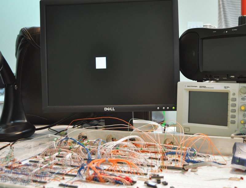
Image
A 400x300 image displayed, and 16 32x32 sprites moving around.

Notice the single pixel white border being drawn over the screen over the image and sprites.
There border proves that all video signals are synced to the clock, and counter properly.

So this proves that the Video System is working perfectly, as well as the GPU switching system.
The next step will be to connect the GPU destination counters and get some sprites moving around.
With only the destination section working, sprites will just be single color square blocks, but this will be enough to prove the system.

Ok, off to cut, strip, and connect another few hundred wires.

Cheers,
Radical Brad


Top
 Profile  
Reply with quote  
PostPosted: Mon Jul 13, 2015 2:06 pm 
Offline
User avatar

Joined: Mon May 25, 2015 2:25 pm
Posts: 690
Location: Gillies, Ontario, Canada
Made some progress last night.
One step forward, but probably going to be two steps back.

Image
Connected the Destinations Counters to the Bus Switch.

I jacked in the Destination side XY counters so that I could test the timing and pathways through the system.
The Destination counters send pixels to the Back Buffer, anywhere on the 400x300 memory.
The counters form a state machine that do a nested for loop. Kind of like this...

Code:
for ( x = 50; x < 150; x++ ) {
for ( x = 60; x < 130; x++ ) {
// Draw pixels from sprite memory to screen at XY, ignoring alpha pixels.
}}


So the 18 bit address bus (9X and 9Y) were connected to the input side of the switch.

Image
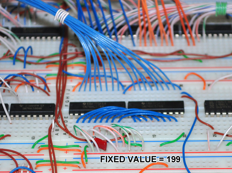
The Pixel Data will be fixed by hard wiring the data input.

In this test, I did not connect the Source counters, as I only wanted to do a basic test.
The Source counters send a serial stream of pixels from the 1024K dedicated graphics memory.
Instead of a bitmap of pixels, I just tied the Data Switch input to the value of 199, which is pure purple.
If the Destination circuit works, then sprites will just be solid purple ugly blocks.

Image
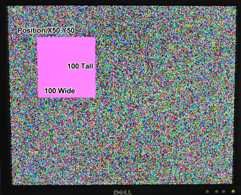
Wow, that ugly block is hard to miss!

Well, after making a simple AVR program to simulate the 6502 setting up the counters, the results were exactly as expected - an ugly purple block on the screen with the expected dimensions and at the expected position. I manually clocked the counters for this test via the AVR clock out pin, but this test did work at 20MHz, so the pathways are all good.

What set me back was the operation of the load pin on the 74HC163 counters.

Seems I miss-read the datasheet a bit. I thought I could send the preset data and then wiggle the LD pin to set the data so that it would register on the next rising edge of the clock (just like the 74HC590 counters).

Nope.

You actually have to send the preset data, drop the LD pin, cycle the clock, and then set the LD pin back to high.... what a cludge!!
I am not going to add another dozen chips to deal with this issue, so I think the 163's are going to go.

I know the 74HC191 and 192 counters are synchronous, but don't suffer from having to manually clock the loaded data.
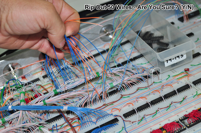
So, it looks like I will issue a "Rip-Up" command, which sends my hand into the board to yank up a handful of wires.

I will study the 163 a bit more, but I don't think it is load friendly, so it is probably going to have to go.

Later,
Brad


Top
 Profile  
Reply with quote  
PostPosted: Mon Jul 13, 2015 3:34 pm 
Offline
User avatar

Joined: Fri Dec 11, 2009 3:50 pm
Posts: 3367
Location: Ontario, Canada
Quote:
Seems I miss-read the [ '163 ] datasheet a bit. I thought I could send the preset data and then wiggle the LD pin to set the data so that it would register on the next rising edge of the clock (just like the 74HC590 counters).

Nope.

You actually have to send the preset data, drop the LD pin, cycle the clock, and then set the LD pin back to high.... what a cludge!!
I am not going to add another dozen chips to deal with this issue, so I think the 163's are going to go.

I know the 74HC191 and 192 counters are synchronous, but don't suffer from having to manually clock the loaded data.

What makes the '590 unusual is the fact it includes a holding register as well as the count register itself. IOW there are 16 flipflops inside, even though it's an only an 8 bit counter. It can remember one 8-bit value while it independently deals with another 8-bit value.

I'm not aware of any other 74 series counters that have a holding register -- the '590 is quite unusual. Be sure you're not confusing the holding-register issue with the question of whether loading is synchronous or asynchronous. That is a separate matter.

Quote:
I will study the 163 a bit more, but I don't think it is load friendly, so it is probably going to have to go.
Unfortunately the 74 series ICs don't offer any better alternative AFAIK. If you really need a holding register I'm afraid it'll require more chips. It's not the 163's fault!

Do you have an up-to-date block diagram you can share with us? I confess I'm rather foggy on how your project is gonna work, although I have no doubt it's clear in your own mind.

-- Jeff

_________________
In 1988 my 65C02 got six new registers and 44 new full-speed instructions!
https://laughtonelectronics.com/Arcana/ ... mmary.html


Top
 Profile  
Reply with quote  
PostPosted: Mon Jul 13, 2015 5:02 pm 
Offline
User avatar

Joined: Mon May 25, 2015 2:25 pm
Posts: 690
Location: Gillies, Ontario, Canada
Both the 192 and 193 counters will load as soon as LD is wiggled, and the next value clocked out is the loaded value.
I understand the 590, and exploit the extra register intensively in this design!

My problem with the 163 requiring a clock pulse after LD is that the Y counter is clocked by the reset of the X counter, so in order to load,
I need extra circuitry to take control of the clock away form the 688 comparator that clocks it on a wrap.

No problem, I already have a plan... use 192 or 193 counters, which do not suffer form this bizarre clocked loading system.
I have used then this way before and the work perfectly.

Here is a brief description of how these counters operate and why I want to be able to load then "off the clock"...

[GPU IDLE MODE]

In this mode, all counters are disabled via count enable, and the output bus is tristated.
To setup for the next sprite copy, the 6502 does these steps through its decode logic...

1) The X1-Destination value are is directly into the counters with a 9 bit value by cycling the LD pins.
2) The Y1-Destination value are is directly into the counters with a 9 bit value by cycling the LD pins.
3) The X2-Destination value is loaded into a 373 that feeds a comparator running form the X1 counter.
4) The Y2-Destination value is loaded into a 373 that feeds a comparator running form the Y1 counter.
5) The Source counters are preloaded to the start address of the sprite data (20 bit address).
6) The Alpha color (transparent) is loaded into a 373 feeding the Alpha logic comparator.

To start a sprite copy, the CPU then cycles a 7474 that is holding the counters count enables off.
If I had to also deal with clock cycling (163) style, this would be a lot more logic to add.


[GPU RUNNING MODE]

As soon as the 7474 is "reset" by the 6502, the counters begin to count at full speed.
The source counters send pixel data directly to to the back buffer through the bus switch, ignoring alpha pixels.

As the X counter reaches its X2 value, the comparator sends the LD signal back to reload the start value X1.
This reset is also the clock line of the Y counter, advancing it to the next line.

When the Y counter reaches its Y2 value, its comparator hits the 7474 and once again disables the GPU counters.
The 6502 peeks at this signal, to know when the GPU is busy.


So as you can imagine, it would be a serious issue to have to send a clock pulse just to preset the counters, which are idle.
This would be especially tricky as the X counter wraps to the X2 value and resets itself back to the X1 value in the 373.

I believe that I can achieve this with minimal fuss using the 192 or 193 counters.
Next session at the loaf of breadboards will prove or disprove this theory.

Brad


Top
 Profile  
Reply with quote  
PostPosted: Mon Jul 13, 2015 6:18 pm 
Offline
User avatar

Joined: Mon May 25, 2015 2:25 pm
Posts: 690
Location: Gillies, Ontario, Canada
Hmmm....

Reading the 163 datasheet in from another company, the wording is slightly different again...

These counters are fully programmable; that is, the outputs
may be preset to either level. As presetting is synchronous,
setting up a low level at the load input disables the counter
and causes the outputs to agree with the setup data after
the next clock pulse, regardless of the levels of the enable
input.


Once again, reading this, I would assume that I could wiggle the LD line, and then let the clock continue on its way.
But in real life, I have found that the ONLY way to preset is do to this...

1) Stop the clock.
2) Drop LD.
3) Cycle the clock.
3) Release LD (high).

Without the clock cycle in there, the counter simply does not load, which is not how the datasheet reads to me.

Brad


Top
 Profile  
Reply with quote  
PostPosted: Mon Jul 13, 2015 6:32 pm 
Offline
User avatar

Joined: Sun Oct 13, 2013 2:58 pm
Posts: 491
Location: Switzerland
Rather than only reading the datasheet you should have a look at the block diagram which clearly shows that changes can occur only using the clock. counting presetting and clearing are synchronous to the clock.

cheers

Peter


Top
 Profile  
Reply with quote  
PostPosted: Mon Jul 13, 2015 6:55 pm 
Offline
User avatar

Joined: Mon May 25, 2015 2:25 pm
Posts: 690
Location: Gillies, Ontario, Canada
Indeed!

Looking at both the block diagram and text on my NXP datasheet, one could see it 2 ways....

1) Synchronous meaning that the actual LD pin change function is synced to the clock.
2) Synchronous meaning that the load happens right away, but the loaded data is sent on the next clock.

I read the posted description as being #2, but in real testing, it worked as #1.

Brad

cbscpe wrote:
Rather than only reading the datasheet you should have a look at the block diagram which clearly shows that changes can occur only using the clock. counting presetting and clearing are synchronous to the clock.

cheers

Peter


Top
 Profile  
Reply with quote  
PostPosted: Tue Jul 14, 2015 12:22 am 
Offline
User avatar

Joined: Mon May 25, 2015 2:25 pm
Posts: 690
Location: Gillies, Ontario, Canada
I promised to post the good, bad, and ugly.
Here is some bad...

Image
Damn 163's! I shall ban you from the board!

I have a handful of 193 counters going into the board instead.
Too bad they are not pin compatible.... DOH!

Oh well, if I wanted easy I would just plug in a Raspberry PI, eh?

Brad


Top
 Profile  
Reply with quote  
PostPosted: Wed Jul 15, 2015 2:36 pm 
Offline
User avatar

Joined: Mon May 25, 2015 2:25 pm
Posts: 690
Location: Gillies, Ontario, Canada
Small update...

Plugged in the 11 new 74HC193 counters, and preliminary testing is looking good.
I can now load the counters by a single pin change, and no longer need an enable pin.
Holding the LD pin low not only loads, but also holds off the counting function (like clock enable).

Next tests will include some ugly purple block sprite tests using the new hardware.

Brad


Top
 Profile  
Reply with quote  
PostPosted: Mon Jul 20, 2015 1:30 am 
Offline
User avatar

Joined: Mon May 25, 2015 2:25 pm
Posts: 690
Location: Gillies, Ontario, Canada
Funny, I started this project as a rainy weekend time filler, and now the weather has been great!
With the GPU almost ready to fire up, I would rather be in my basement lab than out in the back 40, doing homestead work!

With only 2 hours to spare this weekend, I did manage to get 50% of the new GPU system wired up.
Everything from here is just untested napkin theory, but I can't imagine why it wouldn't work on the first power up.
After all, I am using the min propagation values from the datasheet, and have accounted for all timing routes.

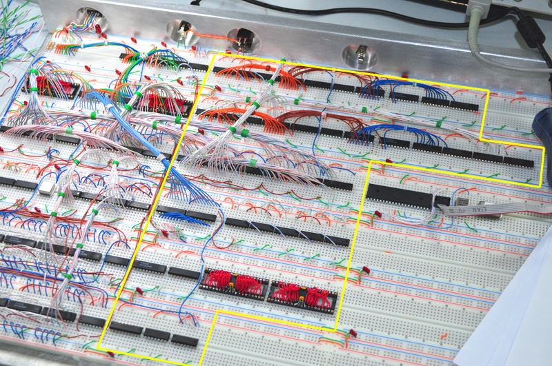
So here is what I have so far. Everything in the yellow border is the new GPU circuit...

Image
42 More Logic Chips Make the New GPU!

The entire board now has 74 Chips... ironic, considering the name Vulcan-74.
Of course, when I am done, I expect the silicon count to be well over 150!
That's more silicon than an episode of Baywatch, dude! Oh wait, that's "silicone", sorry.

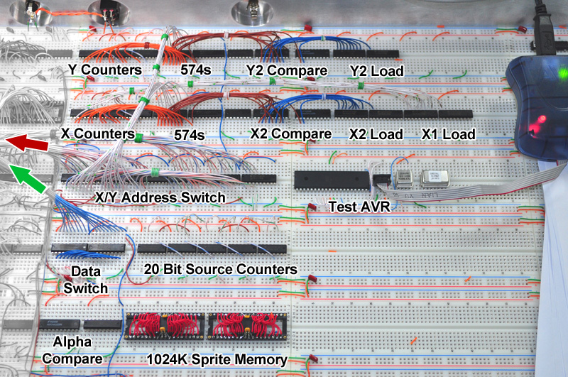
Anyhow, here is a description of what's what in this loaf of breadboards...

Image
It's a growing city of ICs connected by highways of wire.

The entire GPU is on it's own clock domain, and the only signals out are shown by the arrows.
Red is the switched address direct to the back buffer memory, and green is the data.

When Video System is displaying contents of the Live Buffer, the Back Buffer is completely available to the GPU, and invisible to the Video System.
This way, the GPU may write to the memory at its own leisure, at any speed up to 50Mhz, which is my current tested limit.

The AVR is outside the yellow border, as it is also isolated from both the GPU and Video Systems.
AVR will be replaced by 6502 once things are working.

Because the 6502 will live in it's own world, and clock Domain, I fully expect to achieve a working speed of 20MHz.
The 6502 will ONLY connect direct to a 10ns 64K dedicated memory, and all IO will by done using uber-cool trickery.
No ROMS or VIA dinosaurs to slow me down baby, just pure 10ns SRAM to run programs from.

If I have time over the week, I will try to get the rest of the GPU up and running, under AVR test control.
The final goal of the GPU... no less than 64 sprites of 32x32 size moving around at 60 frames per second.
Now remember, these ain't your grand-daddy's C-64 sprites, these are 256 color sprites with built in alpha color!

Cheers out to all 6502 freaks... 8 bits is always enough bits, man!

Radical Brad


Top
 Profile  
Reply with quote  
PostPosted: Thu Jul 23, 2015 10:28 pm 
Offline
User avatar

Joined: Mon May 25, 2015 2:25 pm
Posts: 690
Location: Gillies, Ontario, Canada
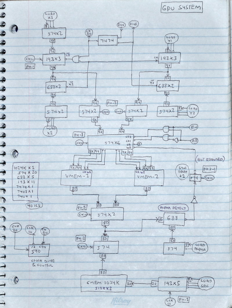
Since I replaced the 163 counters with 193 counters, a small bit of the logic has changed.
Here is an updated "plan of attack" for the GPU circuit I am almost finished laying out...

Image

Currently, I am coding the AVR assembly program that will simulate the 6502 talking to the GPU.
If all goes well, the next update will show some serious pixel magic.
If all goes not so well, then I will post a very colorful image of my fist full of wires again.

Later.

Radical Brad


Top
 Profile  
Reply with quote  
PostPosted: Thu Jul 23, 2015 11:12 pm 
Offline
User avatar

Joined: Thu Dec 11, 2008 1:28 pm
Posts: 10986
Location: England
Block diagram! On paper! Good to see it! (I sometimes think that diagramming is where our computers slow us down most.)


Top
 Profile  
Reply with quote  
PostPosted: Sun Jul 26, 2015 6:13 pm 
Offline
User avatar

Joined: Mon May 25, 2015 2:25 pm
Posts: 690
Location: Gillies, Ontario, Canada
Wow, it's a scorcher out up on that roof! +35 and roofing are a bad mix.
Have to take frequent breaks today, so Vulcan is getting small bursts of attention.

Ok, so I am going to re-adjust the GPU design again, as I am not satisfied with the results.
I will be removing all 574s from the GPU, to make it fully asynchronous (single clock).

Here are the events that lead up to this design change...

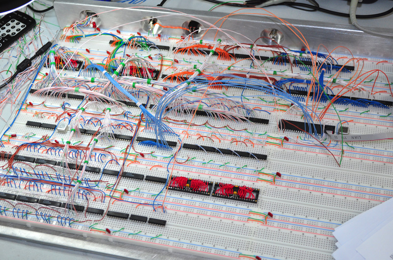
Image
AVR wired up to test the GPU Logic.

I wired up the AVR to simulate both the 6502 control of the GPU as well as the counter reset / reload logic.
This way, I could make sure the address and data paths to the Video System were going to work.

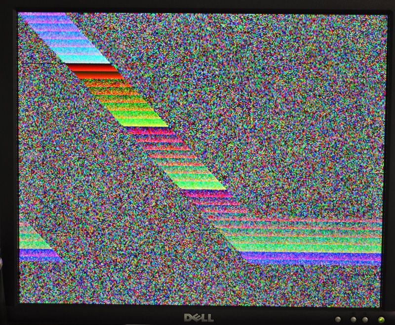
Image
What a colorful mess that was!

I expected to see a 32x32 block move across the screen changing colors on every frame swap.
Forgetting to reload the X-Counter, I ended up with this scrolling mess across the screen.
The good thing is that this was what it should have done having the X-Counter not resetting.
Ok, back to fix up a few missing wires and adjust the AVR assembly code.

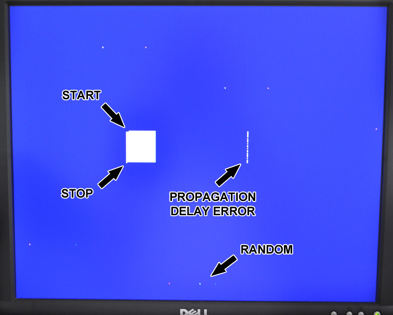
Image
A Scrolling white block with some glitches.

This time I added a Screen Clear routine, which just draws a huge 400x300 blue block to the screen.
From there, the AVR instructed the GPU to draw a moving 32x32 white block to the Back Buffer and then Flip the screens.
I did get the block I expected, but this circuit revealed 4 hardware errors, some not easy to repair.

The first issue was the start and stop of the counters during a reload.
The block starts too late, and continues too long... 2 pixels to be exact.
This was not an unexpected error, since all data has to travel 3 phases through the 574 sequence.
Because of this, I would need to add extra circuitry to kill 2 cycles at the start and then waste 2 cycles at the end.
Hmmm... I didn't like that.

The second issue was a random line that appeared ahead of the block, typically in the same places on the screen.
After some analysis, it was determined that this was the 3rd X-Counter lagging behind on the 9th bit change.
Since all counters are 4 bit, there are 3 counters chained to make the 9X and 9Y address counters.
Having chained counters means propagation through ripply carry, and it was more than I bargained for.
Looking again at the datasheet, each ripple will add 20ns to the count, so I was only getting 70ns output at best.
Ok, this issue was the first trigger to my redesign decision.

The last issue was random pixels being drawn as the block moved across the screen.
I solved this issue, which was cross-talk introduced in a the switched data lines that were wrapped together.
I forgot that when one bank is switched, the Video System still drives signals back to the other, which is in high impedance state.
This issue was fixed by simply bundling the to and from wires apart from one another.
On a real PCB, this would not have been an issue, so that's good.

My new GPU will not have "phases", and contain no 574's. It will drive pixels on a single clock cycle.
Of course, this will come at a clock reduction, but tests and calculations have shown 6.66Mhz to be safe.

Image
Testing a single cycle GPU Idea.

I bypassed the 574's and recoded the AVR assembly to simulate the single cycle GPU Idea.
Everything is left to clock, ripple, and propagate to the Back Buffer, with a window of 150ns.
At 150ns (6.66Mhz), all address and data easily reach the Back Buffer SRAM, but not synchronously.
The slowest path is the WE line, controlled by the Alpha Circuit, followed by the dual 9 bit addresses.

In order to deal with this chaos, WE is held off until the falling edge of the clock, and then asserted.
In some way, this logic is similar to what is needed by the 6502!

In order to optimize speed, I am going to clock a 4017 decade counter by 20MHz, and divide it by 3.
This will give me a 6.66Mhz GPU clock, with the initial high state being 33.3 percent of the cycle.
On the 3rd count, the 4017 resets, and delivers a low clock for 1 third of the cycle, registering the WE line.

Will this work? Yup...

Image
Glitch free moving cube!

With the AVR reprogrammed to simulate the H-H-L 6.66MHz clock, things worked perfectly.
The good news is that the new GPU will have a about a dozen less chips, and be easier to control.
The bad news is that no matter what, I would have to live with 6.66MHz at best due to ripple carries.

This is still 6,666,666 pixels per second, and that's one evil amount of GPU speed man!
This speed will still equate to over 100 bit-mapped 32x32 sprites with 256 colors and transparency.
I think the 6502 will be happy with that kind of graphics performance!

So I have now removed all chips and wires from the GPU side of the board to start from scratch.
Yes... everything right of the Video System has been ripped up!!

No big deal... it's all part of this game! If it was easy, what fun would it be, right?

Not sure when the next update is coming. I have 2 sheds and a chicken coop on the go as well!
Perhaps the rain will send me indoors a few days this week.

Until next time... keep on rockin' in the 8 bit world!

Radical Brad


Top
 Profile  
Reply with quote  
PostPosted: Sun Aug 02, 2015 3:25 pm 
Offline
User avatar

Joined: Mon May 25, 2015 2:25 pm
Posts: 690
Location: Gillies, Ontario, Canada
My time has been very limited lately, but last night Vulcan-74 has made another milestone of progress!
The XY half of the GPU is now working perfectly, complete with Alpha Control.

After seeing the failure of the 574 synced version, I tore up 90% of the GPU to start over.

This time, I lowered the clock, but planned for single cycle operation, using a 6502-like dual phase clock, that in my instance will clock our pixel data on the rising edge, and then do alpha detection and writing to memory on the falling edge.

In order to keep this system as efficient as possible, I clocked a 74HC4017 decade counter, to divide the master 20MHz clock by 4. The clock pulse is taken on the 4th count, which also drives the reset. This clock sequence is then inverted, so I get a pulse stream of HI-HI-HI-LO. This works perfectly, since the counter pathway needs a lot more time than the registering of output data and the WE line. If I were to simple use a 50% duty cycle clock instead, then I would have to divide the master clock even more to give the counters more time before the falling edge.

I will explain this in MUCH more detail when I redo this project on my website as a DIY plan.
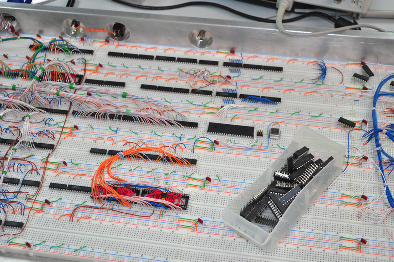
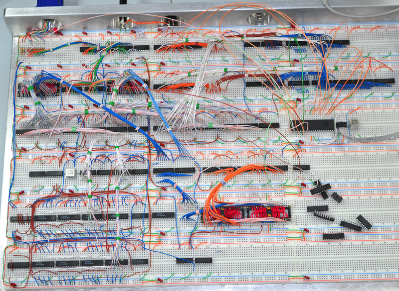
Image
It's a baron waste land of abandoned circuitry!

I ripped up most of the GPU wires, and took out any 74HC574 that was being used as a "phase" to clock data.
Now each of these GPU signals must reach the destination in a single cycle...

- X Destination Sprite Address (9 bits)
- Y Destination Sprite Address (9 bits)
- Pixel Data Destination (8 bits)
- Pixel Data for Alpha Control (8 bits)
- Alpha Comparator WE Line (1 bit)
- Source Sprite Address (20 bits)
- Pixel Data Source (8 bits)

This required a full redesign of the entire GPU with the exception of the 20 bit Source Counters.
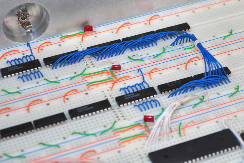
Image
Redoing the XY counter wiring.

Any job worth doing is worth doing right, so I plugged in the new ICs and cut proper length wires.
Dude, we got a lot of wires here!
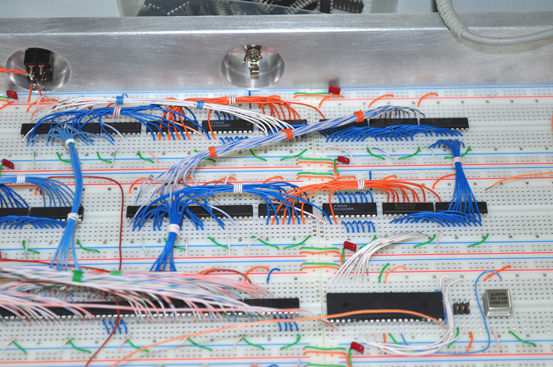
Image
The XY Destination Counter System.

The XY address generation system is much the same as before, using 74HC193 counters and comparators.
The X counter can count from any number between 000 and 399, and the Y counter range is 000 to 299.
The reset of the X counter triggers the Y counter, and the wrap of the Y counter halts the GPU to a "Completed" state.

The 6502 (AVR for now) simply sets the start and end data for the counters and then hits the "Run" line to get them going.
As the GPU does its magic, the 6502 can go on to do other things, and only needs to check that the GPU is done before sending it another command.
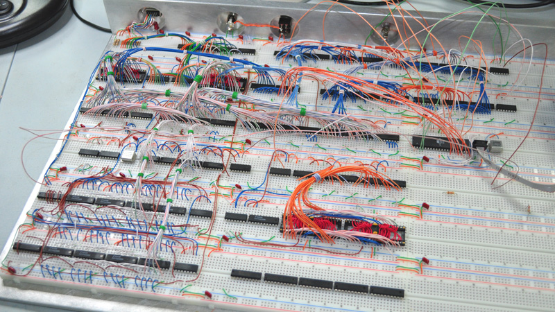
Image
Spaghetti anyone? Temporary wires from the AVR.

The rest of this wiring is a dreadful mess, but that's because it's only temporary.
Since the AVR is only acting as a 6502 stuntman for now, the wiring is just tossed in adhoc.

At this point, only the upper half of the GPU is being tested, so all Sprites will appear as solid blocks.
In order to make them look nicer, this time I added a data port from the AVR to set the color of the blank Sprite Data.

The AVR sets the following 8 bit data bytes and then triggers the GPU to execute the command...

- Destination X1.lo Start Address
- Destination X1.hi Start Address
- Destination X2.lo End Address
- Destination X2.hi End Address

- Destination Y1.lo Start Address
- Destination Y2.lo End Address
- Destination Y2.hi End Address

- Destination Block Color (temporary)
- GPU Run Signal

Once the data is set, the AVR sits back and enjoys a Mojito as the GPU logic fires out pixels like hellfire.
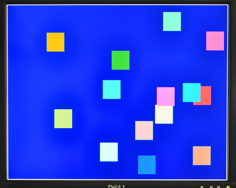
Image
Dummy Sprites generated at 60 FPS by the GPU!

Now, these solid 32x32 blocks may not look that impressive, but this is really a landmark achievement in the GPU design.
Once the Source logic is connected, these Sprites will have 256 colors as well as full transparency using the Alpha Color Control.
Sprites can be any size from 1x1 pixels to 400x300 pixels, and have 255 colors, with one color used as transparency.

Seeing these blocks move around at 60 frames per second glitch free means that the GPU is 100% functional now!!

The GPU is even being used as a temporary "Screen Clear" system by first drawing a 400x300 blue block at location 0,0 on the screen.
From there, the AVR draws 16 randomly bouncing 32x32 Sprites, which at this point only show up as solid blocks.

On a side note, the "Screen Clear System" will be another logic subsystem that simply wipes the entire back buffer to any color.
using 74HC590 counters, I intend to clock this part of the logic to 40MHz. Yes, you read that correctly... 40MHz logic on a breadboard!

The GPU is currently achieving a pixel rate of 5 Million Pixels per Second! Not too bad for a handful of logic chips on breadboard, eh?
Once I verify the operation of the Source half of the GPU, I may try to up the speed to 6.66 MPPS.

Before the GPU was working, the AVR running at 20MHz could manually draw maybe 8 blocks at 60 FPS.
The GPU can easily do 60 or more! The 6502 clocked at 20MHz is going to have similar performance.
Image
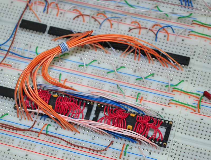
The Source Sprite Memory - next to be connected.

Now that the GPU has been proven, I am hyped to wire up the bottom half and show some real sprites.
I only need to hook up the Source Sprite Memory, which is a 1024k SRAM pair with a 20 bit counter.
Pixel data is streamed our serially to the Alpha Control, in sync with the XY Destination Counter Logic.

For those who are afraid to try a single panel breadboard over 1Mhz, consider this...

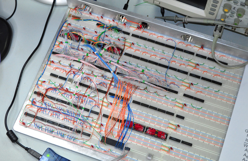
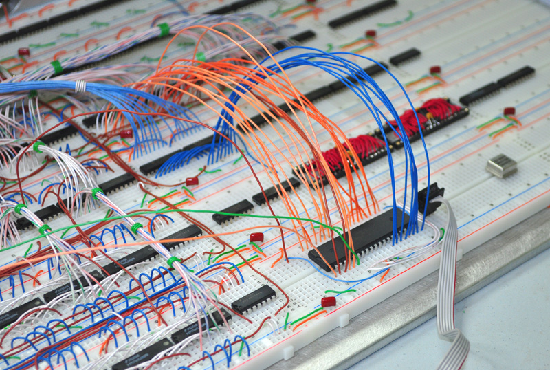
I now have half of this Goliath breadboard hooked up, and it is clocked from single 20MHz oscillator.
There are 80 ICs on the board, and several SRAMs that are being accessed at 20Mhz.
VGA is being drawn to an 800x600 screen at 60Hz, and it is 100% standard exact.
When completed, I will have 24 breadboards tied together running over 150 ICs.
One part of this circuit will be clocked at 40MHz.


If all goes well, the next set of images will have real sprites with transparency moving around the screen.
I have videos as well, but it takes days to upload from my Off-grid, Redneck, Boondocks satellite internet, so maybe later!

Cheers,
Radical Brad

Top
 Profile  
Reply with quote  
PostPosted: Mon Aug 03, 2015 9:10 pm 
Offline
User avatar

Joined: Mon May 25, 2015 2:25 pm
Posts: 690
Location: Gillies, Ontario, Canada
I finally hooked up the Source Memory so I could see if the Alpha Control was working.
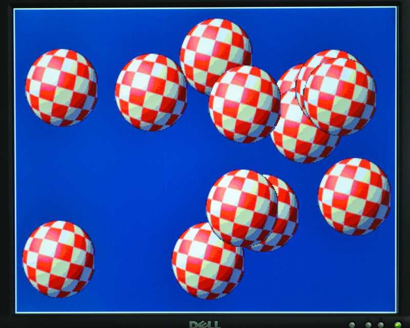
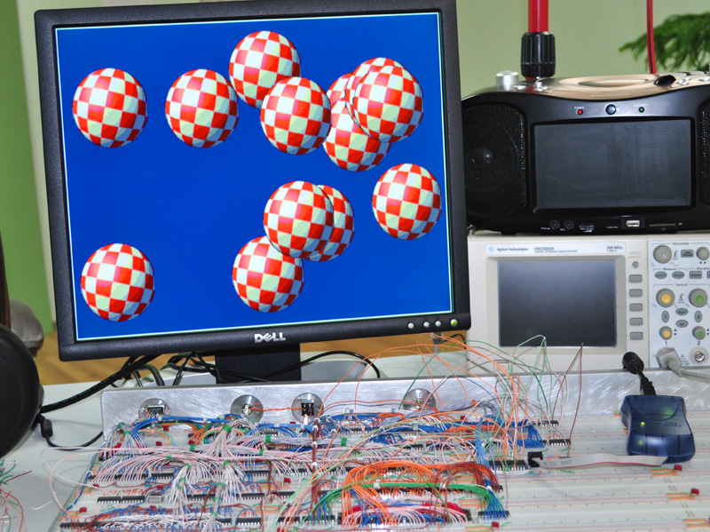
In order to show something a little more impressive than a 32x32 ball, I stole the Amiga Boing animation and converted the graphics to data statements for the AVR. The AVR simply loads the SRAM and then tells the GPU where each ball frame starts and then where to send it to the Back Buffer. There are 16 frames for the checker ball, each having dimensions of 80x80 with 256 colors.

So, how did the GPU work on the first power up? Well, all I can say is... THIS THING'S GOT BALLS!!!!

Yeah, the GPU had no problem at all animating 32 of these Amiga Balls at 60 frames per second!
I am more impressed by this than when I first seen Boing on an Amiga 500... that was only ONE ball!
This board full of 7400 logic chips is hurling out 32 of them, and it's not even running at full bore yet.

What a success so far!
The video is crisp, vibrant, glitch free, and the GPU is fast as hell.

Image
Balls are spinning and moving at 60 frames per second!

At this point, the GPU has to clear the entire 400x300 screen 60 times per second before drawing the next frame of graphics, so this is a lot of overhead. When the GPU is completed, this task will be done by a dedicated counter block (74HC590's) clocked at 40 MHz. This will improve Sprite performance by almost 60%. This thing is going to be a powerhouse!

Image
The GPU is about 90% completed now.

I have about half of the breadboard populated now, and might have enough room for the rest of the circuitry. Going to be tight!
The FastClear circuit will eat another row, and the sound system may need 8 or more full board sections.
Add to this the 6502 decoder logic, and external cartridge loader, and I may be hurting for space!
I will probably only build one of the 4 sound channels, and then wait for the final version to add the other 3.


Here is a video of the 16 Sprites moving around...

Image
https://youtu.be/M9kUlFZM0gM


This was slowed down to only 16 frames per second to capture with my camcorder.
The GPU can actually handle twice as many balls at 4 times the frame rate!!

Ok, off to clean up the wiring mess and make the board look nice again.
Next test will be the 40MHz FastClear circuit.

Once that works, it will be time to install the Pièce De Résistance... 6502!

Cheers,
Radical Brad


Top
 Profile  
Reply with quote  
Display posts from previous:  Sort by  
Post new topic Reply to topic  [ 842 posts ]  Go to page Previous  1 ... 3, 4, 5, 6, 7, 8, 9 ... 57  Next

All times are UTC


Who is online

Users browsing this forum: No registered users and 29 guests


You cannot post new topics in this forum
You cannot reply to topics in this forum
You cannot edit your posts in this forum
You cannot delete your posts in this forum
You cannot post attachments in this forum

Search for:
Jump to: