6502.org Forum  Projects  Code  Documents  Tools  Forum
It is currently Fri Nov 22, 2024 11:50 pm

All times are UTC


Post new topic Reply to topic  [ 842 posts ]  Go to page Previous  1, 2, 3, 4, 5, 6, 7 ... 57  Next
Author Message
PostPosted: Tue Jun 23, 2015 6:13 pm 
Offline
User avatar

Joined: Mon May 25, 2015 2:25 pm
Posts: 690
Location: Gillies, Ontario, Canada
You nailed it!
A few ns of lag and the dreaded fat/skinny first/last pixel issues rears its ugly head.
Not so bad on a glass CRT, but horrible banding on an LCD.
All outgoing signals MUST sync to a clocked register.

Funny, I could probably generate VGA with a handful of 555 timers, one-shots, and some 1970's op amps, but try to make 100% perfect VGA and draw a single pixel border around the edge of the screen (0,0-399,299 in my case) without banding, fuzzng, or thickness variations... now that's another thing altogether! Challenging even on an FPGA so I have found out.

I use the 163's quite a bit in other parts of this project, but in the video addressing circuit, I had to stick to the 590's for reasons I will get into as I detail everything.

I use them in another circuit I call "fast clear" as well, which is clocked at an amazing 50Mhz on this breadboard!
163's didn't like that kind of speed.

Thanks,
Brad


Dr Jefyll wrote:
Quote:
you wouldn't have to use pull-down resistors to hold the low level required during blanking, but alas, there would be another problem.
Right -- that's one of the problems I noticed. The other is that, on '574 (or '273), the prop delay from clock to output will differ from the prop delay from OE\ (or CLR\) to output.

To provide the absolute timing regularity that video demands, it's pretty well obligatory to arrange things so a single clock signal updates both pixel data and blanking.

I would consider replacing the '574 with a pair of '163 counters, which offer synchronous load and synchronous clear, both from a single clock. ('163s are great little chips -- good for so much more than just counting!)

cheers,
Jeff

Top
 Profile  
Reply with quote  
PostPosted: Tue Jun 23, 2015 6:38 pm 
Offline
User avatar

Joined: Fri Dec 11, 2009 3:50 pm
Posts: 3367
Location: Ontario, Canada
Quote:
I use the 163's quite a bit in other parts of this project, but in the video addressing circuit, I had to stick to the 590's for reasons I will get into as I detail everything.
The (8-bit-wide, non-loadable) '590 makes sense for the the video addressing circuit. But for the video output circuit it seems to me a pair of 'hc163s could replace your '574 as well as both of the 'hc08 ANDs. Am I missing something?

I admit the reduction in package count doesn't mean much if you've already got that section wired. But next time you build a Vulcan-74 can wire it that way! :D

Your project looks great -- congratulations!

-- Jeff

_________________
In 1988 my 65C02 got six new registers and 44 new full-speed instructions!
https://laughtonelectronics.com/Arcana/ ... mmary.html


Top
 Profile  
Reply with quote  
PostPosted: Tue Jun 23, 2015 6:52 pm 
Offline
User avatar

Joined: Mon May 25, 2015 2:25 pm
Posts: 690
Location: Gillies, Ontario, Canada
In my design, I gave the counters both tasks; video memory addressing, and as counters to the frame generator FSM. I managed to do this by dividing the horizontal period by 2, which then clocks the vertical period, again divided by 2 by dropping the first bit.

This works out well because I can simply switch blanking periods as the horizontal and vertical counters wrap back to zero.
I send the output of the counter pairs through a set of switched 574s and out to the video memory. This is the dual buffer switching system.
In older systems, I actually had secondary counters for video SRAM addressing, but this new design is "tighter" and has a few less chips.

So the entire video driver circuit (including double buffering) is all controlled by only 4 counters (74HC590).

In my GPU, I use 74HC163 counters exclusively, since they need to be set for X1,Y1,X2,Y2 on the destination (back buffer SRAM) and for 20 bit addressing of the 1024K graphics memory isolated bus.

There are 9 counters in the GPU so far, each running at 20MHz.

I may also add another video memory called "the canvas" that overlays a scrollable background in real-time to the "live buffer" by dropping it under any alpha pixels driven from the video memory being displayed. This would offer some serious game-field scrolling capabilities that go far beyond typical tile engines.

Speaking of counters, the sound system has 5 x 74HC163 counters for every channel, and I am thinking 4 channels split into stereo pairs.
No doubt, the logic that will stuff the 65C02 program memory and other SRAMs on startup will also have a fist full of counters.

Thanks to this project, NXP will have to open a new production line for DIP parts!

Brad

Dr Jefyll wrote:
The (8-bit-wide, non-loadable) '590 makes sense for the the video addressing circuit. But for the video output circuit it seems to me a pair of 'hc163s could replace your '574 as well as both of the 'hc08 ANDs. Am I missing something?

I admit the reduction in package count doesn't mean much if you've already got that section wired. But next time you build a Vulcan-74 can wire it that way! :D

-- Jeff


Top
 Profile  
Reply with quote  
PostPosted: Tue Jun 23, 2015 7:30 pm 
Offline
User avatar

Joined: Mon May 25, 2015 2:25 pm
Posts: 690
Location: Gillies, Ontario, Canada
Sorry, I missed your reply... thanks!
A few answers...

The 6502 is actually not aware of the video system at all. In fact, it cannot see any other memory besides it's own dedicated fast 64K SRAM. For this reason, programming the 6502 will be easy - no interrupts or timing to worry about. The 6502 doesn't even need to be synchronous to the other clock, and I may bump it back up to 25MHz later on.

The Video System is self contained. It runs without the need for the 6502. In fact, in a few days, it will power up and show 120,000 random pixels from either of the SRAM banks. I will post a video of swapping banks by dropping a single IO line high or low.

The GPU is a real GPU as far as the definition goes. It will be able to move memory blocks from a dedicated 1024K of SRAM back to the video system onto whatever buffer is no "live" at the time, which is the "back buffer". The 6502 simply asks the GPU to do something and then goes on its way without having to wait. Perhaps the 6502 can go and talk to the Sound Processor while the GPU is busy moving a 125x200 sized 256 color sprite to the back buffer.

The GPU sees the video memory (destination) as a set of X and Y locations, but sees the dedicated graphics memory (source) as a contiguous stream of 1024K. The GPU is also "alpha aware", meaning that any selected single color out of the 256 available can be ignored, or seen as transparent to the video memory. In typical game programming, you need to "save and restore" the video memory as graphics are drawn, but in this system, the GPU spares the user from this torture.

Hope that makes some sense!

Ps... 24 units in this board!

Cheers!
Brad


cbscpe wrote:
Quote:
This is also why I can't see the reason to use EEPROM in a 65C02 project these days when for a few cents, you can pre-load a fast SRAM and do away with all the wonky propagation issues and slow clocks needed to support 150ns technology, not to mention having to dredge up an expensive programmer.


That's exactly what I think is the easiest way for a fast system. I had my share with slow (90ns) EEPROMs and the problem when setting up a system the first time, especially the iteration of pulling the EEPROM, putting it into the programmer and then back. Only to find out that you only found the second last error in your monitor.

It's impressive to see the fast progress you make even with the rules you have put onto yourself and the type of circuits you're using, and how neatly you are laying out your cables. When I do my breadboard projects they are first not half the size of your MoBB, the maximum I use is 5 units and you have this 18-unit monster. I also like the trick adding intermediate latches to avoid problems with the propagation delay with many stages of signal processing. It's almost like a modern CPU with pipelines.

Hope to see the first real video output.

One question I have, when you talk about GPU I suppose it is more a CRTC for VGA signals as you do all video data calculation in the CPU? Is that correct?

cheers

Peter


Top
 Profile  
Reply with quote  
PostPosted: Tue Jun 23, 2015 8:48 pm 
Offline
User avatar

Joined: Fri Dec 11, 2009 3:50 pm
Posts: 3367
Location: Ontario, Canada
It's all good, and I envy you being able to indulge in a project like this. 8) What I was referring to was more basic, though -- simply the notion of replacing this
Attachment:
vsch1_.jpg
vsch1_.jpg [ 63.09 KiB | Viewed 3561 times ]
with this:
Attachment:
vsch1_(rev).jpg
vsch1_(rev).jpg [ 39.24 KiB | Viewed 3561 times ]
In this application the '163s "counters" don't count in any way -- they are used simply as edge-triggered registers, featuring the synchronous load and synchronous clear modes we require.

It takes a pair of 163s to implement the 8-bit register, but I didn't bother to explicitly draw both 163s. The power and control pins all go in parallel; only the data IO pins are separate. The CET and CEP inputs can be tied either high or low; the thing won't ever count anyway because the load & clear functions both override the count function (and clear overrides load).

The only potential problem I can see is if one '163 happened to be significantly faster or slower than the other (I don't think a slight difference would matter). Luckily, for a project like yours it's acceptable to hand pick your parts. As long as both 163s are from the same vendor -- the same lot, even -- I expect that'd resolve any issue. But it's always possible there's something else I'm missing.

cheers,
Jeff

_________________
In 1988 my 65C02 got six new registers and 44 new full-speed instructions!
https://laughtonelectronics.com/Arcana/ ... mmary.html


Top
 Profile  
Reply with quote  
PostPosted: Wed Jun 24, 2015 12:38 am 
Offline
User avatar

Joined: Mon May 25, 2015 2:25 pm
Posts: 690
Location: Gillies, Ontario, Canada
Hey, thanks for the idea of using a 163 as register with clear... never thought of that one!
It's like learning a new op code!

Although this will certainly come in useful at some point, there is an issue driving the DAC from a 163 as I have found out in a different test. As you mentioned, pathways are not perfect through each of the 4 bits, and this shows as slight phasing on some monitors that have to self adjust. So I would still need one more 574 after the 163's, which puts me back to the same chip count as the 2 AND gates.

But I will be using this idea elsewhere, so thanks for posting this!

Cheers!
Brad


Top
 Profile  
Reply with quote  
PostPosted: Sun Jun 28, 2015 1:51 am 
Offline
User avatar

Joined: Mon May 25, 2015 2:25 pm
Posts: 690
Location: Gillies, Ontario, Canada
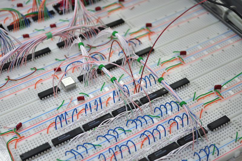
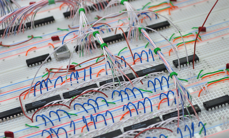
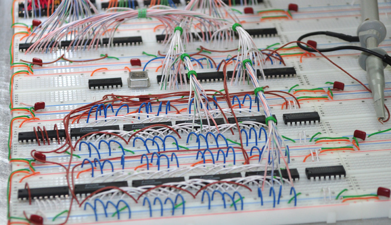
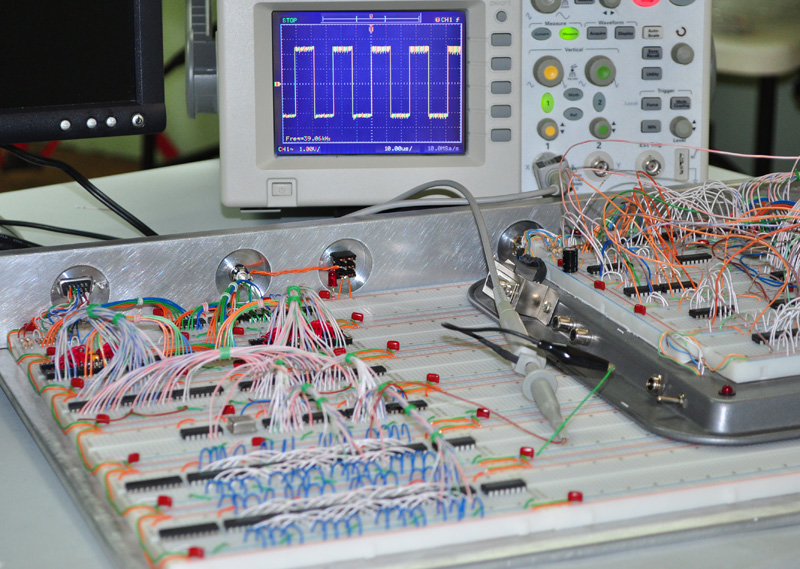
After a long day of yard work, I decided to relax in my cool basement lab and mess around on the Vulcan-74 board for an hour.

Image
With all of the comparators and address counters wired up, I hit the switch and started probing the board.
The vertical counter is resetting at 60Hz, which is exactly what was expected.
Notice how much neater the new board is compared to the original test mess.

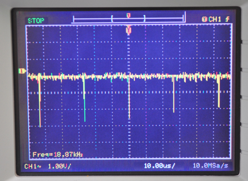
Image
Probing the comparator output for the horizontal line reset.

Image
This is the vertical refresh timing divided by two... perfect.
The pulse is sharp since it is low for only 1 out of 528 cycles.

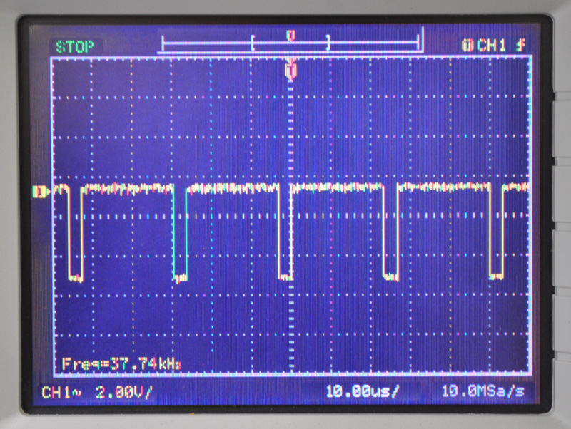
Image
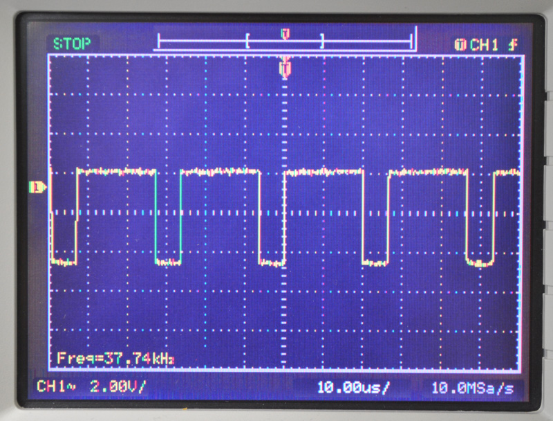
This is the flip-flop that controls the horizontal sync pulse.

Image
Horizontal sync is active when the pulse is low.

Image
This is the flip-flop that controls the horizontal blanking period.

Image
The high time is when horizontal pixels are dawn.
Once again, timing works out exactly to the 800x600 VGA standard.

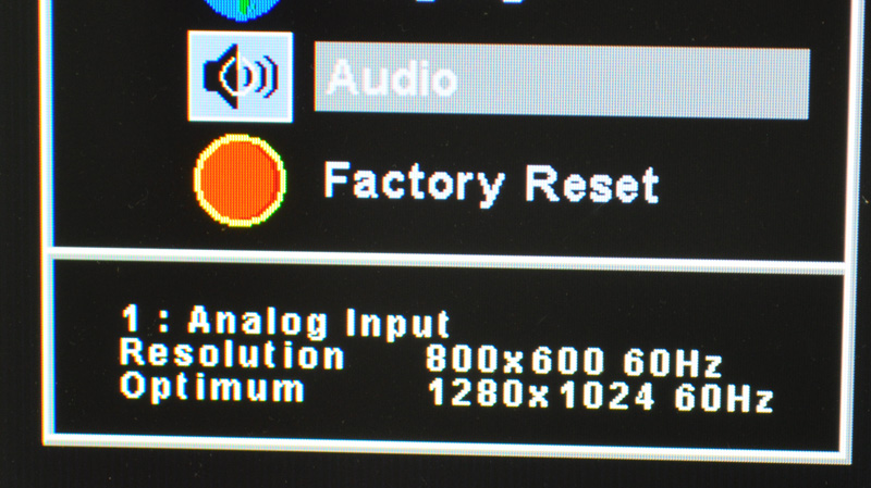
Image
With the sync pulse logic working, the monitor locks on to the 800x600@60Hz standard.
This monitor is native at 1280x1024, so there will be a 1.6 to 1.0 clock phase adjustment.
At my final resolution of 400x300, this phasing is hardly noticeable.

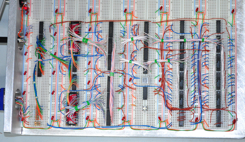
Image
This is the entire dual buffer video system with all wiring cleaned up.
The video board is capable of driving a monitor without any external control.
Of course, the SRAM will contain only random pixels at this point.

Image
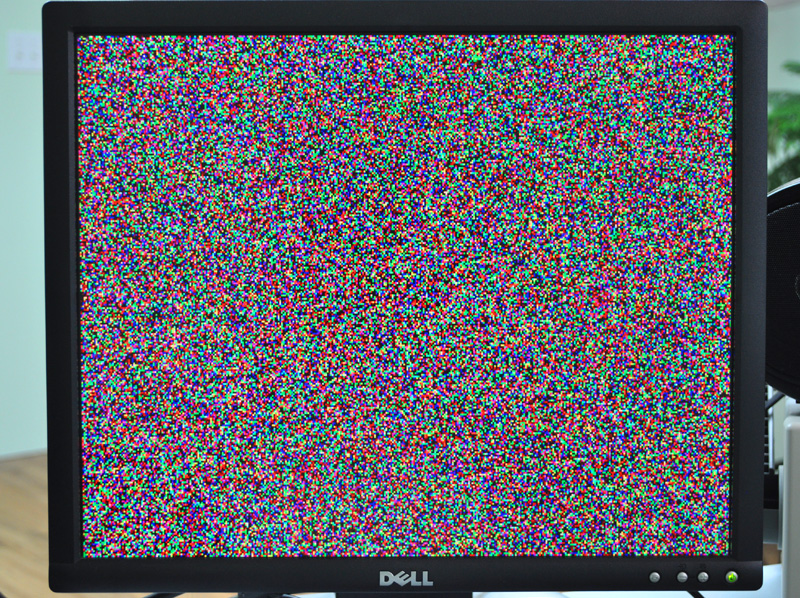
Speaking of random pixels, here they are in vibrant 256 colors.
Each bank of SRAM contains 120,000 pixels, with seamless buffer switching.
The banks are swapped on the vertical sync pulse so there as no banding or tearing in video.
Double buffering means the CPU can draw to one bank while the other is being sent to the screen.
The non-live bank can by accessed as if it were completely disconnected from the video logic.

VGA from a handful of common logic chips ans some SRAM... yeah baby!

Image
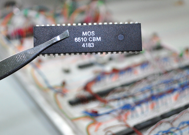
Soon I will be plugging my favorite processor into the board!
Ok, I am not using a MOS variant, but I did have to give it a glory shot!

The next stage of Vulcan-74 design will be the ultra fast GPU logic, which will eat up at least one more column on the board.
The GPU has its own independent 20 bit address bus, and 1024K SRAM at 10ns, where it will store "sprites".
My GPU design is kind of like an Amiga Blitter on steroids. I will deal with XY blocks, not just lines of pixels.
Alpha (transparent) pixels are also built into the GPU, so the programmer won't have to do slow XOR tricks on graphics.

Ok, that's all for now, I will try to post a video of the bank switching if I have time tomorrow.
Until the next rainy day....

Radical Brad


Top
 Profile  
Reply with quote  
PostPosted: Sun Jun 28, 2015 4:42 am 
Offline
User avatar

Joined: Thu Dec 11, 2008 1:28 pm
Posts: 10986
Location: England
Bravo!


Top
 Profile  
Reply with quote  
PostPosted: Sun Jun 28, 2015 9:18 am 
Offline

Joined: Wed Sep 11, 2013 8:43 pm
Posts: 207
Location: The Netherlands
Sheer beauty!!!

You realise that you have to make block diagrams and schematics etc. for the rest of us? :shock:

_________________
Marco


Top
 Profile  
Reply with quote  
PostPosted: Sun Jun 28, 2015 12:57 pm 
Offline
User avatar

Joined: Mon May 25, 2015 2:25 pm
Posts: 690
Location: Gillies, Ontario, Canada
Thanks all!

I intend to make a 300-400 page E=book showing every step of the design from breadboard to final board, including schematics, testing procedures, source codes, pcb design (possibly) and several windows programs to convert sound and graphics into EEPROM data. The final design will even include instructions on a retro style cabinet and DIY C64 style joysticks.

The entire book will be available on my website and as a downloadable PDF. No costs for anything, of course!
Just my way of giving back to the community, and hopefully sparking some interest in retro technologies.

Brad


lordbubsy wrote:
Sheer beauty!!!

You realise that you have to make block diagrams and schematics etc. for the rest of us? :shock:


Top
 Profile  
Reply with quote  
PostPosted: Sun Jun 28, 2015 1:45 pm 
Offline
User avatar

Joined: Thu Dec 11, 2008 1:28 pm
Posts: 10986
Location: England
That would be great - especially if you include missteps and mistakes and false leads!


Top
 Profile  
Reply with quote  
PostPosted: Sun Jun 28, 2015 1:57 pm 
Offline
User avatar

Joined: Mon May 25, 2015 2:25 pm
Posts: 690
Location: Gillies, Ontario, Canada
Those could make an entire chapter!
Sometimes the mishaps are just plain funny.

The other night, I was up too late and ripped up a bunch of wires to try something new, but it failed completely.
I actually considered using "undo" for a second! Yeah... you know you need sleep when!

Brad

BigEd wrote:
That would be great - especially if you include missteps and mistakes and false leads!


Top
 Profile  
Reply with quote  
PostPosted: Sun Jun 28, 2015 10:37 pm 
Offline
User avatar

Joined: Mon May 25, 2015 2:25 pm
Posts: 690
Location: Gillies, Ontario, Canada
Here is a quick video tour of the VGA System...

Image
https://youtu.be/nQtSusVWgk4

Next tests will be done with an ATMega-1284, drawing images to the screen.
Once the images tests are passed, the GPU logic will be prototyped.
The 6502 will then replace the AVR, leaving nothing but 7400 series logic on the board.
The sound system will be the last thing to be made, once again 100% pure logic.

No point calling something Vulcan-74 unless it lives up to the name!

Brad


Top
 Profile  
Reply with quote  
PostPosted: Fri Jul 03, 2015 2:14 pm 
Offline
User avatar

Joined: Mon May 25, 2015 2:25 pm
Posts: 690
Location: Gillies, Ontario, Canada
The weekend is here, and if I get rained out of my construction project, then the chips shall fall (or at least get plugged into the breadboard).

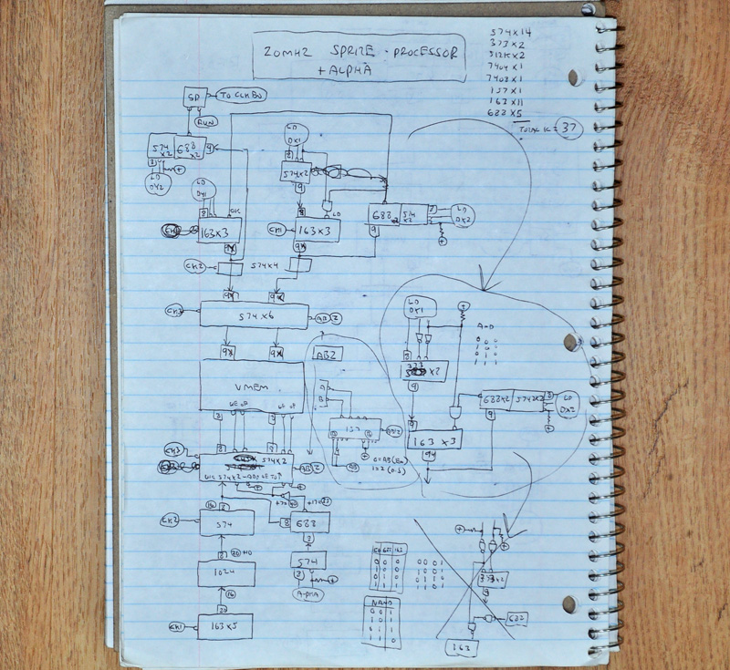
I have given my 20 MHz GPU system some serious thought and ran it through an intensive simulation process (AKA - 5 minutes and a sheet of paper)...

Image

Yeah, this is about as much pre-work I do on these projects!
I prefer to hit the board rather than mull over why something might not work.
The best simulator is a prototype, dude! Don't fear the "real World".

Anyhow, here is the plan as per the chicken-scratch above...

A 10 nanosecond bank of 1024K of memory (Graphics Memory) runs on its own isolated 20 bit address bus, fired by a series of 163 counters clocked at 20Mhz.
This is contiguous memory holding the "sprite data". The CPU can preset set the 163s with 20 bits of "Source Address".
The GMEM is clocked through 3 stages, with a series of 574s that keep propagation below 40ns, and allow switching to the dual buffer Video Memory.
As pixel data is pumped out of the GMEM, it is qualified with a known value set in the 688 comparator by the CPU, which is called "Alpha Color".
Any data NOT equaling Alpha, is sent to the VMEM data port, registered in sequence with the address and WE, controlled by the Alpha logic.
Data equaling the Alpha Value is considered "transparent", and is not drawn. This is how the GPU handles automatic transparent pixels at 20MHz.

On the "Destination" side of the logic, we have a split set of chained 163 counters running the X and Y address counters to the VMEM back buffer.
The CPU presets these values; Destination-X1 and X2, Destination Y1 and Y2. This tells the GPU where on the screen to draw the sprite block.
As you can see, sprites are not limited in any way, and can be as small as a single pixel, or as large as 512x512 due to the 9 bit XY addressing.
A few 688s control the resetting and wrapping of XY counters, and then trigger a "Ready" signal at the end of a sprite transfer.

By using this GPU, the 6502 can just set a few bytes and then go on its way as the GPU moves massive sprites around the screen at 20 million pixels per second!

Here is a best case comparison of drawing a 32x32 sprite to the back buffer using the GPU and the 6502 only...

Video -> 1 full frame @ 60 Hz lasts for 331,584 cycles @ 20 Mhz
6502 -> Optimized assembly loop @ 40 cycles per pixel = 40,960 cycles = 8 Sprites
GPU -> 1024 cycles @ 20 MHz = 323 Sprites

So if the 6502 could actually run at 20MHz, it could only send 8 sprites per frame as compared to 323 sprites drawn by the 37 logic chips in the GPU!!

And since the 6502 need only hurl out a few bytes to setup the GPU, it may only need 50 cycles of time before it can move on to other game tasks.
With the GPU having an independent dual bus, the 6502 could go onto game logic or doing sound tasks while the GPU is running... no waiting around!

So that's my plan.
I will start hammering in chips sometime this weekend, depending on the flow of cloud juice.

Cheers,
Radical Brad


Top
 Profile  
Reply with quote  
PostPosted: Fri Jul 03, 2015 2:40 pm 
Offline
User avatar

Joined: Thu Dec 11, 2008 1:28 pm
Posts: 10986
Location: England
Excellent - I love block diagrams, they can convey so much more than code or schematics or text.

Edit: so your GPU gives you the equivalent horsepower of an 800MHz 6502. That's a new record!


Top
 Profile  
Reply with quote  
Display posts from previous:  Sort by  
Post new topic Reply to topic  [ 842 posts ]  Go to page Previous  1, 2, 3, 4, 5, 6, 7 ... 57  Next

All times are UTC


Who is online

Users browsing this forum: No registered users and 43 guests


You cannot post new topics in this forum
You cannot reply to topics in this forum
You cannot edit your posts in this forum
You cannot delete your posts in this forum
You cannot post attachments in this forum

Search for:
Jump to: