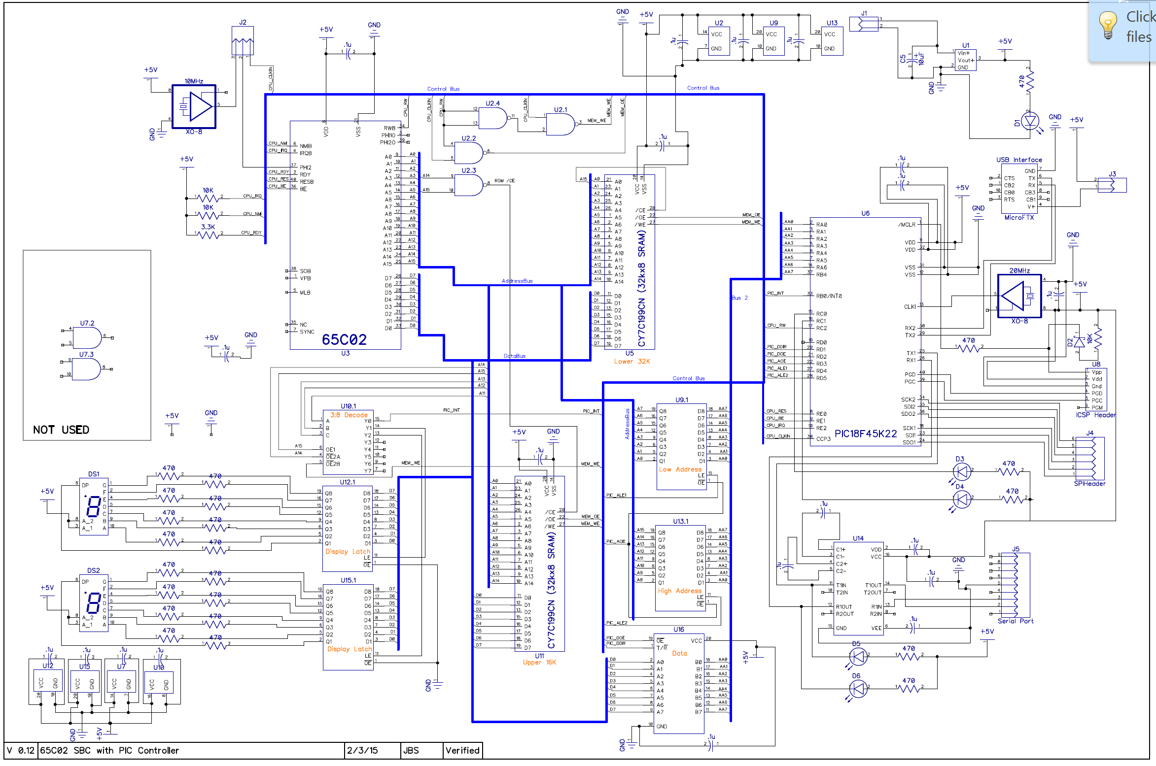
I am just about to do the routing for a PCB construction my first 65C02 SBC (using OSH Park which happens to be here in Portland). I was inspired by a few of the SBCs here on 6502.org, in particular the work by phvic and the ERIC-1 (
viewtopic.php?f=12&t=3103) and Michael's mini PCB design (
viewtopic.php?f=1&t=2854).
My design is somewhat similar to those designs in that I am using a PIC microcontroller as both the 'bootloader' as well as the 'interface' device.
In my particular case I am planning of the following:
(1) The PIC will generate the primary clock and reset inputs for the 65C02. This could run the 65C02 at up to 10MHz, or as slow as DC. Since I am using a 65C02 the PIC can also use the BE pin to disable the CPU outputs.
(2) The 65C02 will have 32K of SRAM at 0x0000-0x7FFF, and 16K of SRAM (simulating ROM) at 0xC000-0xFFFF.
(3) For diagnostic purposes I have two 7 segment displays off of a 3:8 decoder at 0x8800 and 0x9000.
(4) At start up, the PIC will put the correct code into the upper SRAM chip, then fire up the 65C02.
(5) For communication from/to the 65C02 and the PIC:
The 65C02 will write to a predefined memory buffer in the upper SRAM, and let the PIC know there is data there by writing 0x8000 (which will trigger the 3:8 decoder output to the PIC Interrupt pin)
The PIC will write to a memory segment in the upper SRAM when data needs to be returned to the PIC, and let the 65C02 know using the 65C02 interrupt pin.
By using the 'shared' SRAM for communication, I can have buffered data in both directions, multiple command sets, etc.. Easy to expand in software.
For the PIC to be able to read or write to the upper and lower SRAM, it will need to pause the 65C02 CPU and use the BE pin to tri-state the bus lines from the 65C02. You can see the AND gates right before the MEM /WE and MEM /OE pins going to the SRAMs. Those AND gates allow the PIC to either control those lines, or pass through what the 65C02 is doing.
Unlike a few of the other designs, I am only using 8 digital IO lines on the PIC for address and data, so I added 3 latch/buffers. This gives me more lines on the PIC for other devices. I have two serial ports, plus two SPI ports pulled out. I suspect I will use the SPI ports for keyboard and display connections.
The schematic mentions a 'MicroFTX', which is a small board that has the surface mount serial to USB chip plus the USB connection already mounted. They can be found here:
http://jim.sh/ftx/ Here is a PNG of the schematic:

And here is a link to a PDF of said schematic:
http://www.sponaugle.com/post/65C02SBCSchematic.pdfAs well as the DIPTrace schematic:
http://www.sponaugle.com/post/6502SBCMainBoard_V0.12.dchI still need to add decoupling caps, and power and ground to some of the ICs. Once that is done, I'll quickly do the routing and get some boards made.
I'll post up the fully routed board, all files need to get PCBs made, complete parts manifest, and all of the source code and compiled code to get it working.
I'm looking for any comments/ridicule/that wont works/etc! Anything look wonky?
Cheers,
Jeff Sponaugle


