6502.org Forum  Projects  Code  Documents  Tools  Forum
It is currently Fri Nov 01, 2024 2:26 am

All times are UTC


Post new topic Reply to topic  [ 21 posts ]  Go to page 1, 2  Next
Author Message
PostPosted: Tue Feb 03, 2015 9:11 pm 
Offline

Joined: Sat Jan 10, 2015 3:14 am
Posts: 13
(first post, so be nice!)

I am working on a small 65C02 based SBC, using some elements that are similar to a number of other 6502.org members approach of using a PIC/AVR to provide bootloading of the ROM.

I had a question about the timing requirements as it relates to a memory write. Assume I am talking only about the WDC65C02, not the older MOS 6502s.

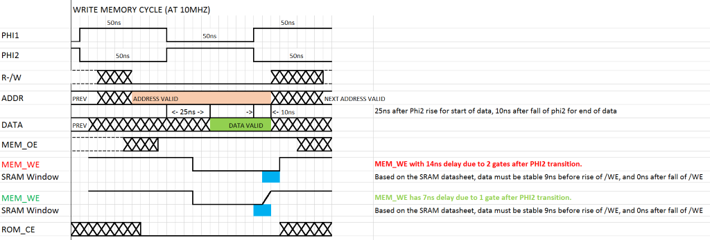
First, a simple timing diagram. Increments (cells) are 5ns apart.
Image

In looking at the datasheet for the 65C02, during a write cycle the output data lines are guaranteed to be active and valid at least 30ns before the fall of phi2, and 10ns after the fall of phi2. That is represented in the diagram in green. These are minimum values, and there are no listed maximum values.

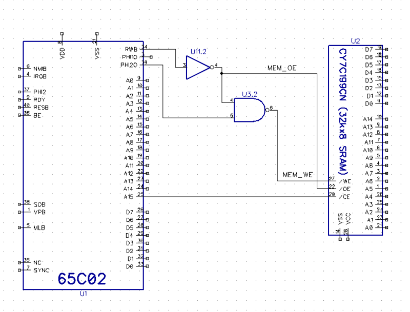
Consider the simple (incomplete, just for discussion) circuit below:
Image

Let's assume for discussion that propagation delay through a gate is 7ns. (74HCT)

In this circuit, the /WE pin on the SRAM is controlled by the NAND of Phi2 and /RWB (inverted RWB). That is also represented in the first timing diagram as MEM_WE in green. In this configuration, when Phi2 transitions happens, the SRAM will see the rising of /WE 7ns later. For this particular SRAM, the data has to be valid 10ns before the /WE rising transition, and 0 (ZERO) ns after the transition. In this case, there would be no problem. The SRAM effectivly clocks the data on the rising edge of /WE, but needs no hold over ( I would assume due to internal propagation in the design.)

All is good.

Consider an addition where I want to be able to read and write from that same SRAM via my PIC controller while the CPU is paused. Assume for this conversation that the CPU can be paused, and the BE raised such that the 65C02 will tristate it's output pins.

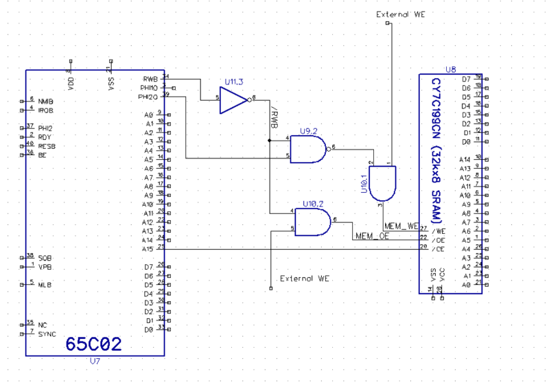
I first proposed the following circuit:
Image

In this circuit, I added an additional AND gate in front of both the MEM_WE and MEM_OE signals. This would allow these external lines to control the memory (by going to 0), or let the CPU signal pass through (by going to 1). The downside of this approach is that it adds an additional gate delay to the signal AFTER the falling edge of Phi2. This is represented in the timing diagram as MEM_WE red. Since the two gates would add up to 14ns of delay, the rising edge of MEM_WE that the SRAM sees will happen 4 ns after the CPU data lines could potentially go invalid.

It is possible that this might just work, as the 10ns of data hold time is the minimum listed in the 65C02 datasheet... but I have no experience to say if that is true. It is interesting that this effect is not related to cpu clock speed, as the 10ns data hold time is a fixed value (at 5V)s. The only limitation is the delay from PHI2 to the SRAMs /WE.

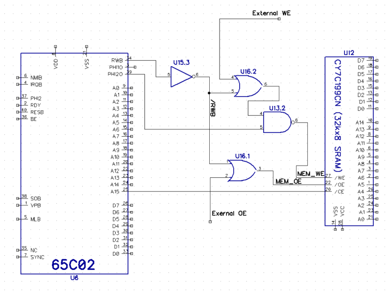
An alternate fix is to consider this:
Image

In this circuit I have moved the external AND gates behind the gates that mix in Phi2. In this case the falling edge of PHI2 is only delayed by one gate (7ns), thus the memory write pattern should work correctly. The only problem is that for this design to work, the 65C02 must be paused with the PHI2 in the high state, and the External OE and WE are inverted ( 0 - pass through, 1 - PIC assert ).

Is there anything obvious that I am missing here?

Jeff


Top
 Profile  
Reply with quote  
PostPosted: Tue Feb 03, 2015 10:08 pm 
Offline
User avatar

Joined: Fri Aug 30, 2002 1:09 am
Posts: 8534
Location: Southern California
If all the loads are CMOS, the hold time will be potentially milliseconds or more, not just microseconds or nanoseconds, after the processor stops driving the bus; so you don't have to worry about that part. The time when write data becomes available needs to be referenced to the rising edge of phase 2 though, being no more than a maximum guaranteed time after the rise. Where it is relative to the fall of phase 2 then depends on the half-cycle time.

Jeff Laughton has some good animated, to-scale timing diagrams at http://laughtonelectronics.com/Arcana/V ... iming.html .

_________________
http://WilsonMinesCo.com/ lots of 6502 resources
The "second front page" is http://wilsonminesco.com/links.html .
What's an additional VIA among friends, anyhow?


Top
 Profile  
Reply with quote  
PostPosted: Wed Feb 04, 2015 1:49 am 
Offline

Joined: Sat Jan 10, 2015 3:14 am
Posts: 13
GARTHWILSON wrote:
If all the loads are CMOS, the hold time will be potentially milliseconds or more, not just microseconds or nanoseconds, after the processor stops driving the bus; so you don't have to worry about that part. The time when write data becomes available needs to be referenced to the rising edge of phase 2 though, being no more than a maximum guaranteed time after the rise. Where it is relative to the fall of phase 2 then depends on the half-cycle time.

Jeff Laughton has some good animated, to-scale timing diagrams at http://laughtonelectronics.com/Arcana/V ... iming.html .


I can see that if I use the BE pin to disable the outputs that the loads will have long hold time, but I was more concerned with a CPU controlled write followed by a CPU controlled read, where the write data hold timing is close to the minimum hold time. Of course now that I think about it, a write cycle followed by a read cycle will be very similar, as the CPU will tri-state the data lines for input.... which will certainly give the SRAM plenty of hold time. A write followed by another write will also have plenty of time given the write output doesn't change until the rise of phi2.


Yea you are right about the write data (from the CPU) being 'available' on the databus is referenced from the rise of Phi2, and the datasheet specifies that as 25ns. If the clock cycle were so fast that that minimum SRAM setup time could not be met I would have problems. I see what you mean about where the 'start of data available' is relative to the fall of phase 2.. as the clock rate increases you will have less data setup time to give to the SRAM. That is a great point. Fortunately that isn't an issue with a 10MHz clock and SRAM I selected, since the setup time needed is only 9ns before latch.

I had seen those animated diagrams and they make the changes in clock timing very clear. Good stuff.

Since my only issue was the delay of the /WE signal to the SRAM relative to the databus changing for the next access cycle, I think this is going to work fine.

If I really need to have a complex (and high delay) path for the /WE to memory path, I could always put a buffer in front of the SRAM. That would add propagation delay to the data lines.. of course that makes the setup time more of a limit, but there is plenty of margin there.

Thanks for the input. Very helpful.

Cheers,

Jeff


Top
 Profile  
Reply with quote  
PostPosted: Wed Feb 04, 2015 2:38 am 
Offline

Joined: Sat Jan 10, 2015 3:14 am
Posts: 13
Oh.. and I updated that timing picture I posted to reflect the two timing constraints from the datasheet for the 65C02, plus the window the SRAM needs.

Image


Top
 Profile  
Reply with quote  
PostPosted: Wed Feb 04, 2015 8:11 pm 
Offline
User avatar

Joined: Thu May 28, 2009 9:46 pm
Posts: 8467
Location: Midwestern USA
sponaugle wrote:
(first post, so be nice!)

Please reduce the size of your images so the screen doesn't have to be laterally scrolled. Better yet, post them as attachments.

Thanks!

_________________
x86?  We ain't got no x86.  We don't NEED no stinking x86!


Top
 Profile  
Reply with quote  
PostPosted: Wed Feb 04, 2015 8:58 pm 
Offline
User avatar

Joined: Thu May 28, 2009 9:46 pm
Posts: 8467
Location: Midwestern USA
sponaugle wrote:
Consider the simple (incomplete, just for discussion) circuit below:...

Some observations for your consideration:

  1. All timing in your circuit should be referenced to the Ø2 clock generator, whose output is applied to pin 37 of the 65C02. The outputs at pins 3 (Ø1O) and 39 (Ø2O) should not be used, per WDC recommendations. Note that Ø1O and Ø2O slightly lag Ø2, which can lead to subtle timing errors at higher clock speeds. Ø1O and Ø2O should only be used in cases where the 65C02 is being used to replace the NMOS 6502 in a circuit that was designed for the latter.

  2. Your read/write logic seems to be too complicated. Here's how I did it in my POC unit, which uses a larger version of the SRAM you are using, as well as other devices requiring discrete /RD and /WD signals:

    Attachment:
    File comment: "Universal" read/write generation
    rw_generation.gif
    rw_generation.gif [ 19.57 KiB | Viewed 6018 times ]

    The above circuit fully qualifies RWB with Ø2, an essential requirement when non-65xx devices are attached to the 65xx bus. Note that 65xx I/O devices are slaved to the Ø2 clock and must see RWB and valid chip selects before Ø2 rises during a valid read/write cycle. That is, you must directly connect RWB to the equivalent inputs on 65C21, 65C22 and 65C51 devices, and must ascertain that chip selects on those devices are asserted before Ø2 goes high.

  3. Negating BE will put the 65C02's address bus, data bus and RWB output into the high-Z state, but will not stop the MPU. You would also need to negate RDY to actually stop the 'C02.

  4. 74HCT logic is not recommended in an all-CMOS design (the 'T' in HCT means TTL-compatible inputs). Most 74HCT devices are slower than their 74HC equivalents. Generally speaking, 74HC logic is only slightly faster than 74LS, which will limit the maximum Ø2 rate. I recommend that you use 74AC logic if you are intent on operating your unit at 10 MHz or higher. Aside from substantially shorter prop times, 74AC has more fanout than 74HC, which helps to compensate for the effects of parasitic capacitance.

As Garth notes, parasitic capacitance will cause signal states to persist for a while if everything on the bus goes high-Z. Most designs do not intentionally create such a condition—something is always driving the buses, so you have to be careful about depending on such an effect.

_________________
x86?  We ain't got no x86.  We don't NEED no stinking x86!


Last edited by BigDumbDinosaur on Thu Feb 05, 2015 5:42 am, edited 1 time in total.

Top
 Profile  
Reply with quote  
PostPosted: Wed Feb 04, 2015 11:36 pm 
Offline

Joined: Sat Jan 10, 2015 3:14 am
Posts: 13
BigDumbDinosaur wrote:
sponaugle wrote:
(first post, so be nice!)

Please reduce the size of your images so the screen doesn't have to be laterally scrolled. Better yet, post them as attachments.

Thanks!


Sorry about that... I sometimes forget that an image on my screen that looks about the right size, with 3200x1800 resolution, will be huge on other peoples screen.

I shrank the images down to about 800x600 or so.

Jeff


Top
 Profile  
Reply with quote  
PostPosted: Wed Feb 04, 2015 11:58 pm 
Offline
User avatar

Joined: Thu Jun 23, 2011 2:12 am
Posts: 229
Location: Rancho Cucamonga, California
BigDumbDinosaur wrote:
[*]Your read/write logic seems to be too complicated. Here's how I did it in my POC unit, which uses a larger version of the SRAM you are using, as well as other devices requiring discrete /RD and /WD signals:

Attachment:
rw_generation.gif


Correct me if I'm wrong, but I think most (if not all?) SRAM chips will allow you to keep the /RD line LOW (active) and control the chip with just the /CE and /WR inputs. You would use an address decoder (e.g. 74*138 or in case of a 32K chip, the A15 line) to activate the chip with /CE, and you would use the top of BigDumbDinosaur's circuit to combine RWB and PHI2 into the /WR signal. The NAND port at the bottom of that schematic isn't needed.

For simplicity I use a single SRAM chip in my designs, and I let the microcontroller read the address lines and generate the signal for the /CE input of the SRAM chip). 64KB chips are surprisingly hard to find (except on places like eBay), so my SRAM chip of choice is the Alliance AS6C1008-55PCN, it's a 128KB SRAM chip in a PDIP chip (SMD is available too) and it has a 55ns access time which I think makes it capable of working at the full 14MHz that the WDC 65C02 is spec'd at (I'd have to go over the math again to make sure, though; I only run my 6502's at 1MHz). It works at 5V but also at much lower voltages (I think all the way down to 2.5V, it also has a sleep mode that makes it retain its data -- read the datasheet). And I let my microcontroller control the A16 line so I can decide later to implement some sort of memory swapping/banking scheme.

Quote:
[*]Negating BE will put the 65C02's address bus, data bus and RWB output into the high-Z state, but will not stop the MPU. You would also need to negate RDY to actually stop the 'C02.


If you use the microcontroller to generate the clock for the 65C02, you can also stop the clock instead of pulling RDY low. The 65C02 will even stay off the data bus if you stop the clock in LOW state. However, unless you pull BE down, the 6502 always uses the address bus, even when the clock is stopped!

===Jac


Top
 Profile  
Reply with quote  
PostPosted: Thu Feb 05, 2015 12:55 am 
Offline
User avatar

Joined: Fri Aug 30, 2002 1:09 am
Posts: 8534
Location: Southern California
sponaugle wrote:
Sorry about that... I sometimes forget that an image on my screen that looks about the right size, with 3200x1800 resolution, will be huge on other peoples screen.

3200?? <choke, choke> I've never heard of more than 2000! I think mine is 1600 or so.

_________________
http://WilsonMinesCo.com/ lots of 6502 resources
The "second front page" is http://wilsonminesco.com/links.html .
What's an additional VIA among friends, anyhow?


Top
 Profile  
Reply with quote  
PostPosted: Thu Feb 05, 2015 1:49 am 
Offline

Joined: Sun Jul 28, 2013 12:59 am
Posts: 235
GARTHWILSON wrote:
sponaugle wrote:
Sorry about that... I sometimes forget that an image on my screen that looks about the right size, with 3200x1800 resolution, will be huge on other peoples screen.

3200?? <choke, choke> I've never heard of more than 2000! I think mine is 1600 or so.

While my new years resolution was 1400x1050x24bpp, I'm expecting to get a machine with a 2880x1800 display or thereabouts in a couple of months. But yeah, such display resolution is fairly recent and isn't cheap. And here I am, thinking that trying to get 256x240x1bpp out of a 6502 might take some doing! (which should drag us somewhere at least close to on-topic.)


Top
 Profile  
Reply with quote  
PostPosted: Thu Feb 05, 2015 3:42 am 
Offline

Joined: Sat Jan 10, 2015 3:14 am
Posts: 13
BigDumbDinosaur wrote:
Some observations for your consideration:

  1. All timing in your circuit should be referenced to the Ø2 clock generator, whose output is applied to pin 37 of the 65C02. The outputs at pins 3 (Ø1O) and 39 (Ø2O) should not be used, per WDC recommendations. Note that Ø1O and Ø2O slightly lag Ø2, which can lead to subtle timing errors at higher clock speeds. Ø1O and Ø2O should only be used in cases where the 65C02 is being used to replace the NMOS 6502 in a circuit that was designed for the latter.


*Thank you* for pointing that out.... I skipped over that recommendation in the datasheet, so you saved me a lot of headache! Changing the schematic now.

BigDumbDinosaur wrote:
  • Your read/write logic seems to be too complicated. Here's how I did it in my POC unit, which uses a larger version of the SRAM you are using, as well as other devices requiring discrete /RD and /WD signals:
    Attachment:
    rw_generation.gif

    The above circuit fully qualifies RWB with Ø2, an essential requirement when non-65xx devices are attached to the 65xx bus. Note that 65xx I/O devices are slaved to the Ø2 clock and must see RWB and valid chip selects before Ø2 rises during a valid read/write cycle. That is, you must directly connect RWB to the equivalent inputs on 65C21, 65C22 and 65C51 devices, and must ascertain that chip selects on those devices are asserted before Ø2 goes high.


  • Interesting. Part of my complication comes from wanting to also have the PIC able to drive the /OE and /WE ( /RD and /WR in your diagram ) of both of the SRAMS if the 65C02 is paused. Without that additional logic, my memory circuits would look like:

    Image

    which is even simpler. However your comments made me realize that if I pause the 65C02 (which is easy to do from the PIC since it is controlling the clock), and I use the BE pin to tristate the 65C02, the RWB pin will be tristated... so I can just hook my PIC directly into the same pin on the logic gates. Inside the PIC I can tristate my outputs before starting up the clock again. That removed he need for that extra set of AND gates I added.

    I'll make that change to the circuit.

    It is interesting that in your circuit you have the RWB and the PHI2 going into an NAND gate before going to the SRAM, while I have the RWB just being inverted before going into the SRAM. The difference is of course that in my setup, the /OE pin of the SRAM will remain driven (=0) until the RWB line goes low (as would be the case if the next operation was a write). In looking at the datasheet for the SRAM, if the /CE line is still active (say the next instruction is also a read from the same chip), the output data pins of the SRAM will never tristate.

    This mode is supported in the SRAM. In this configuration, if we assume the CPU is going to read from several hundred address in a row that are all in the same SRAM (say 100 NOPs), the RWB line will *never* go low and by extension the /OE pin and /CE lines will stay at 0 the entire time. The only changes will be to the address lines. I would assume that some SRAMS might actually need activity on the /OE line, but this one will work fine with no transitions at all (for reads).

    This would lead me to believe that it is not needed to NAND the Phi2 and the RWB, no?

    BigDumbDinosaur wrote:
  • Negating BE will put the 65C02's address bus, data bus and RWB output into the high-Z state, but will not stop the MPU. You would also need to negate RDY to actually stop the 'C02.


  • Ah yes.. fortunately since I control the clock from the PIC, I can just pause the whole thing!

    BigDumbDinosaur wrote:
  • 74HCT logic is not recommended in an all-CMOS design (the 'T' in HCT means TTL-compatible inputs). Most 74HCT devices are slower than their 74HC equivalents. Generally speaking, 74HC logic is only slightly faster than 74LS, which will limit the maximum Ø2 rate. I recommend that you use 74AC logic if you are intent on operating your unit at 10 MHz or higher. Aside from substantially shorter prop times, 74AC has more fanout than 74HC, which helps to compensate for the effects of parasitic capacitance.

  • As Garth notes, parasitic capacitance will cause signal states to persist for a while if everything on the bus goes high-Z. Most designs do not create intentionally such a condition—something is always driving the buses, so you have to be careful about depending on such an effect.


    Great input... in looking at the specs those ACs are a bit faster as well, so no reason not to use them. Since I am doing a PCB and not wirewrap, I suspect I can keep the noise down.

    Thanks for the great input.... I'll make another pass at the schematic and fix some of the issues.

    Jeff


    Top
     Profile  
    Reply with quote  
    PostPosted: Thu Feb 05, 2015 3:49 am 
    Offline

    Joined: Sat Jan 10, 2015 3:14 am
    Posts: 13
    GARTHWILSON wrote:
    sponaugle wrote:
    Sorry about that... I sometimes forget that an image on my screen that looks about the right size, with 3200x1800 resolution, will be huge on other peoples screen.

    3200?? <choke, choke> I've never heard of more than 2000! I think mine is 1600 or so.

    I know... The changes in screen resolution over just the last year has been amazing. This is on my laptop, which is a new Dell Precision 3800. It has two different optional screens, once that is 1920x1080, and one that is 3200x1800. Given that it is a 15" screen, that is a lot of DPI.

    My desktop has a Dell UP3214Q display which is 3840x2160, but that is spread out over a 32" screen, which seems much more reasonable.

    Cheers!

    Jeff


    Top
     Profile  
    Reply with quote  
    PostPosted: Thu Feb 05, 2015 4:59 am 
    Offline

    Joined: Sat Jan 10, 2015 3:14 am
    Posts: 13
    I updated my SBC schematic to reflect changes to the read/write logic using the suggestions from above.

    This is how I have the /OE and /WR logic now:

    Image

    I moved to use the CLKIN instead of the Phi2 Output from the 65C02, and I have the /OE NANDed with the CLKIN. You can't quite see it on this picture, but the 65C02 clock input comes from the PIC microcontroller.

    In order for the PIC to read and write from the SRAM, it will stop the 65C02 while the CPU_CLKIN is low, pull BE low, the drive the address, data, and CPU_RWB lines as needed.

    Entire schematic PDF here: http://www.sponaugle.com/post/65C02SBCSchematic.pdf

    Jeff


    Top
     Profile  
    Reply with quote  
    PostPosted: Thu Feb 05, 2015 5:47 am 
    Offline
    User avatar

    Joined: Thu May 28, 2009 9:46 pm
    Posts: 8467
    Location: Midwestern USA
    jac_goudsmit wrote:
    Correct me if I'm wrong, but I think most (if not all?) SRAM chips will allow you to keep the /RD line LOW (active) and control the chip with just the /CE and /WR inputs.

    Some do, some don't. Only the data sheet knows for sure. :lol:

    There is a "gotcha" with keeping /RD low at all times with the 65C816. During a valid memory cycle when Ø2 is low, the '816 emits the bank address. Therefore, continuously asserting /OE on anything will cause bus contention when the device is selected in a read cycle. Hence the circuit you see.

    Incidentally, the 53CF94 SCSI controller requires that /RD and /WD be mutually exclusive. My circuit meets that requirement.

    _________________
    x86?  We ain't got no x86.  We don't NEED no stinking x86!


    Top
     Profile  
    Reply with quote  
    PostPosted: Thu Feb 05, 2015 6:33 am 
    Offline
    User avatar

    Joined: Thu May 28, 2009 9:46 pm
    Posts: 8467
    Location: Midwestern USA
    sponaugle wrote:

    I printed the schematic on B-size paper so I could read it and noted a few things:

    1. The SOB input on the 65C02 must be tied to Vcc or Gnd if you are not planning to actively drive it. Allowing it to float will make it susceptible to noise and may cause the V bit in the status register to be randomly set. There's no telling what that might do in your software. I suggest pulling SOB up to Vcc through a 3.3K resistor so you can use it as a high speed input if desired.

    2. The pullup resistor values for /IRQ and /NMI are too high. I recommend no more than 3.3K for these resistors. If they are too high, a long R-C time-constant will be created and the corresponding circuit will take too long to return to Vcc when all interrupt sources are cleared. Such behavior is a common cause of spurious interrupts. Garth Wilson has a good discussion of this phenomenon in his interrupts article on his website.

    3. I see that you are using an SRAM as a pseudo-ROM, but it appears that it isn't write-protected once the ISL has been completed. A bug in your code could corrupt its contents.

    4. I notice that your serial port has no provisions for hardware handshaking. That will limit its useful speed to around 9600 bps, as XON/XOFF handshaking is unreliable above that speed.

    Otherwise, it looks as though it ought to work once you get the PIC programmed.

    _________________
    x86?  We ain't got no x86.  We don't NEED no stinking x86!


    Top
     Profile  
    Reply with quote  
    Display posts from previous:  Sort by  
    Post new topic Reply to topic  [ 21 posts ]  Go to page 1, 2  Next

    All times are UTC


    Who is online

    Users browsing this forum: Google [Bot] and 12 guests


    You cannot post new topics in this forum
    You cannot reply to topics in this forum
    You cannot edit your posts in this forum
    You cannot delete your posts in this forum
    You cannot post attachments in this forum

    Search for:
    Jump to: