6502.org Forum  Projects  Code  Documents  Tools  Forum
It is currently Tue Apr 30, 2024 4:47 pm

All times are UTC


Post new topic Reply to topic  [ 4 posts ] 
Author Message
PostPosted: Thu Jan 15, 2015 6:55 pm 
Offline

Joined: Thu Dec 10, 2009 1:27 am
Posts: 5
Location: Sunnyvale, CA
Hi everyone, I'm back to trying to figure out the internal structure of the 6502 chip, and I thought I'd ask a question about how data gets to the ALU. Does anyone know if the ALU has input registers or not? When looking at Hanson's block diagram, there are clearly two items labeled "A input register (AI)" and "B input register (BI)" that feed into the ALU. However, when I check the Balazs transistor-level schematic, I don't see anything that resembles a register going into the ALU; it seems like the ALU gets its inputs directly from the internal buses.

I've been trying to figure out how you even WOULD make a register which can receive data from two buses at once. Hanson's block diagram shows that the B input register can store the contents of either the data bus (DB) or the low address bus (ADL). This is simple enough to do with tri-state buffers if the two buses just go directly to the ALU (well, directly through a tri-state buffer), but I actually don't know of any type of register chip that can make use of multiple input lines for each bit. Is there any type of D flip-flop (which is basically what a register is made of) that could actually be made to selectively take its data from multiple inputs? Normally when trying to do something like this, you'd use a multiplexer, but I don't see anything resembling a multiplexer anywhere in the inputs to the ALU, and I doubt that that's what the 6502 actually uses. Can anyone shed some light on this? Thanks!


Top
 Profile  
Reply with quote  
PostPosted: Thu Jan 15, 2015 7:47 pm 
Offline
User avatar

Joined: Thu Dec 11, 2008 1:28 pm
Posts: 10793
Location: England
Long time no see - welcome back.

Visual6502 is my usual go-to reference, but in almost all cases Balazs' schematic will have the same circuits.

You're right to be looking for D-type latches - in MOS technology they are normally just a single pass transistor on the input to an inverter. The inverter's input acts as a capacitor, so when the pass gate is off the state of charge is preserved.

If the latch has several multiplexed inputs, there's no need for a separate mux, because a set of pass gates all connecting to the same storage node acts to provide a set of inputs with their respective enables.

If the output of the latch is to be used to drive some simple logic gate, it may be possible to merge the logic gate with the latch: the storage node is now an input to the logic gate. If two logic gates must be fed by the latched output, one possibility is to duplicate the latch function, and have each gate offer a capacitive input as a storage node, another is to use both of the inputs as the storage node.

And that's what we see with the A and B inputs to the ALU: two or three inputs come in, go through some pass gates, and connect to the inputs of two logic gates which form the first part of the ALU: there's an inverter to provide optional inversion, and a NAND and a NOR to perform logic operations and to form part of the full adder function.

Attachment:
File comment: Clip from Balazs' schematic: ALU inputs with data flowing right to left.
6502-ALU-inputs.png
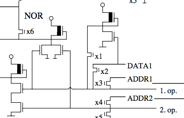
6502-ALU-inputs.png [ 20.27 KiB | Viewed 1652 times ]


Note that Balazs' schematic has the ALU at the top with the output at the left, whereas visual6502 has the ALU at the bottom with the output at the right. Balazs' terms the three input busses DATA1, ADDR1 and ADDR2, whereas visual6502 terms them idb (Internal Data Bus), adl (Address Bus Low) and sb (Special Bus). The five input controls which Balazs' calls x1 through to x5 are called in visual6502 dpc8_nDBADD, dpc9_DBADD, dpc10_ADLADD, dpc11_SBADD and dpc12_0ADD - these names derive from Hanson's naming, which is direct from MOS themselves, via their schematics.

Attachment:
File comment: Visual6502 screenshot of ALU inputs with data flowing left to right
visual6502-ALU-inputs.png
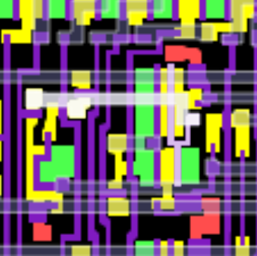
visual6502-ALU-inputs.png [ 70.45 KiB | Viewed 1652 times ]


I've highlighted the B input here. All of that highlighted area is one node, at the same voltage, but the bulk of the capacitance holding the charge is formed by the two transistor gates over on the right: the polysilicon gates run vertically here, and the upper transistor is the input to a two-input NOR gate while the lower one is an input to a two-input NAND gate. There are three logic gates visible: you see the red pullup area for each one. The one on the left is the optional input inverter.

Hope this helps.
Ed


Last edited by BigEd on Fri Jan 16, 2015 11:59 am, edited 2 times in total.

Top
 Profile  
Reply with quote  
PostPosted: Thu Jan 15, 2015 11:18 pm 
Offline

Joined: Thu Dec 10, 2009 1:27 am
Posts: 5
Location: Sunnyvale, CA
Wow, that was a more detailed answer than I was expecting to see. Thank you very much. :)

Now I remember what I'd forgotten: That the 6502 makes relatively extensive use of "dynamic registers," which as you say work just like DRAM: They need to be constantly refreshed. I didn't even think of a transfer gate and a two-transistor inverter as something you could build a register out of, but I see what you mean. If they can hold their charge for one clock cycle, that's good enough.

This presents some problems for people who want to build 6502 replicas using other circuitry. I imagine that what I could end up doing is using the same signal to enable a buffer and D latch; a D flip-flop wouldn't do since it would be edge-triggered, and the edge might trigger before the buffer output has fully propagated to the register, but a D latch would probably work fine.

Thank you again very much for your detailed explanation and information. I'm so glad that we're able to understand the 6502 at this level of detail... It would be a shame to leave its workings a mystery. Cheers!


Top
 Profile  
Reply with quote  
PostPosted: Fri Jan 16, 2015 11:46 am 
Offline
User avatar

Joined: Thu Dec 11, 2008 1:28 pm
Posts: 10793
Location: England
Those three resources - Hanson's diagram, Balazs' schematic, and the visual6502 team's interactive simulation - have been hugely helpful in understanding the chip!

It's true though, that understanding a two-phase design based on transparent latches everywhere is a bit of a challenge - many of us were taught a strict discipline of using edge-triggered registers everywhere. If you have two latches in series clocked on different phases, you have in effect a full edge-triggered register, but in the case of the 6502 there are generally some logic gates, with attendant delay, between every pair.

The other barrier to modelling or rebuilding the 6502 based on the NMOS implementation is the two sets of bidirectional pass transistors which connect the Special Bus in one case to the Address Bus High internal bus, and in the other case to the Internal Data Bus. (A possible way through is to add some extra logic which determines the directionality at any given time.)

Glad to be able to help.
Ed

[I've tweaked a few details in my post above]


Top
 Profile  
Reply with quote  
Display posts from previous:  Sort by  
Post new topic Reply to topic  [ 4 posts ] 

All times are UTC


Who is online

Users browsing this forum: No registered users and 31 guests


You cannot post new topics in this forum
You cannot reply to topics in this forum
You cannot edit your posts in this forum
You cannot delete your posts in this forum
You cannot post attachments in this forum

Search for:
Jump to: