cr1901:
Just as the title suggests... is there any information on the hardware internals of the '02/'816 pipeline beyond the 2 paragraphs in the programmer's manual?
There's not a lot of detail available regarding the cycles in the execution of an instruction for these processors. As you've probably already concluded, a lot of effort will be required to establish the kind of data you are looking for from those two paragraphs and the stated timings of the instructions. While documenting the behavior of my synthesized FPGA processor core, the M65C02, I developed a spreadsheet that contains a map of the opcodes, a cross-reference of the opcodes sorted by addressing modes, and a table of the cycles each opcode requires for execution in my core. You may find it useful. A GitHUB wiki page presenting and discussing the contents of this table can be found
here. The MS Excel spreadsheet can also be found the GitHUB repository for the project, but I dare not point you to it since it might raise BDD's hackles regarding
incompatible industry standard file formats. 
This is of course assuming the '02/'816 pipeline works akin to the Execution Unit and Bus Interface Unit separation of the 8086/8088... A very good example of a string of simple instructions which actually takes longer to execute than a single complex instruction is
SHL ax, 1 vs SHL ax, cl: SHL ax, 1 empties the instruction queue faster than it can be replenished.
The '02, 'C02 and '816 are not pipelined. The '02 and 'C02 certainly don't break down the bus interface and execution units in the manner of the 8086/8088. Given the pedigree of the '816, I doubt that it is partitioned into bus interface and execution units in the manner of the 8086/8088. With bus interface and execution units, the '02/'816 instruction stream can be fetched sequentially and achieve some measure of pipelining as was achieved in the 8086/8088. However, the 8086/8088 BIU simply fetches sequential locations from the instruction memory. It does not perform any of the complex effective address calculations required by the '02/'816 architectures. I suspect that the benefit of prefetch queue to the '02/'816 would be negated by the indirect addressing modes, which are not included in the 8086/8088 architecture, and which are often used by programmers of the '02/'816.
As pointed our here (or on another thread), a rudimentary amount of overlapped instruction fetch and execution is provided. Perhaps it may be more clearly stated to say that the these processors try to overlap the instruction fetch and write back phases of an instruction's execution.
The REP modifier, although problematic with respect to interrupts, should be applied to instructions such the '186/'188 string move instructions. That addition to the x86 ISA is very much worth the increased complexity. The improvement in instruction timing is high, and it certainly relieves the issue that you refer to relative to the prefetch queue. Since the instruction is no longer fetched from memory, the full bandwidth of the processor's bus is available for the move operations.
Basically, I ask because while I was looking at the number of bytes/clocks required for an '02/'816 instruction, I realized something: If neither of those processors were pipelined, each Direct/Zero Page instruction would always save 2 cycles (1 fetch + 1 execute) over a "normal" instruction.
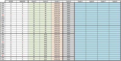
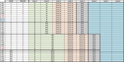
I don't agree with your conclusion regarding the number of cycles that may be saved by an unpipelined '02/'816. I have pasted in two instruction timing tables below. The first shows the instruction cycles for the simple ZP read-only and write-only addressing modes, and the second shows the instruction cycles for the ZP read-modify-write addressing modes. The column labeled
Fetch and the column labeled
Next represent the memory/instruction cycles than can be overlapped. As can be seen from the first figure, the M65C02 and the 65SC02 are able to overlap most these cycles to report the same number of memory/instructions cycles. The 1 cycle difference reported for the zp,X and zp,Y addressing modes comes from the fact that I included a separate address generator in my implementation of the '02/'C02 ISA that allows the M65C02 to make the indexed calculation directly as the next output address is being generated. (This approach works well in an FPGA using high-speed asynchronous memory, but not so much with synchronous RAM.) In neither addressing mode is there an opportunity, in a von Neumann memory architecture, to save two instruction cycles for ZP variables. This is more obvious in the second figure which highlights the instruction cycles for ZP read-modify-write operations. In the second figure, the M65C02 has eliminated one "dead" cycle, and can perform an operand read immediately followed by a ALU result write cycle. A standard '02/'C02 must perform the ALU operation after the operand read cycle, and therefore creates a "dead" memory cycle. (The most significant improvement between the '02 and 'C02 is that the 'C02 reads the source operand address during the internal "dead" cycle instead of writing to the destination address twice as is done by the '02. This improvement, in general, allows the RMW instructions of the 'C02 to be used with R/W control registers of memory-mapped I/O devices. Again, this is not a generally recommended programming practice for memory-mapped I/O devices. Since the M65C02 does not include the dummy read cycle, its RMW instruction behavior can be used with R/W control registers of memory-mapped I/O devices.)

- M65C02 zp; zp,X; and zp,Y Instruction Cycles

- M65C02 RMW zp; and zp,X Instruction Cycles
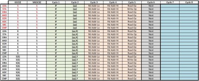
Edit: the following figure was inadvertently loaded rather than the preceding figure. MAM

- M65C02 (zp); (zp,X); and (zp),Y Instruction Cycles
Michael A.