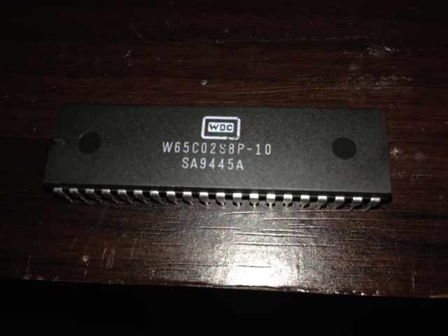
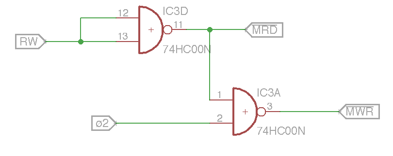
Does the 6502 jump to the Interrupt vector if it encounters things like stack overflows etc?
I've got some simple code just to write to the ACIA but instead of running in a loop, most of the time it just loops in the ISR.
Randomly resetting a bunch of times eventually gets it working, but I have no idea why.
Here's my code that I've managed to bodge together from other examples:
Code: Select all
.PSC02
.SEGMENT "ROMCODE"

ACIA        = $D110
ACIA_CTRL   = ACIA+3
ACIA_CMD    = ACIA+2
ACIA_SR     = ACIA+1
ACIA_DAT    = ACIA

RESET:		CLD             ;Clear decimal arithmetic mode.
			CLI
			LDA #$1E        ;* Init ACIA to 9600 Baud.
			STA ACIA_CTRL
			LDA #$0B        ;* No Parity.
			STA ACIA_CMD
			LDX #$FF

LOOP:
			LDA #$4D
			STA ACIA_DAT    ;*Send it.
WAIT:		LDA ACIA_SR     ;*Load status register for ACIA
			AND #$10        ;*Mask bit 4.
			BEQ    WAIT    ;*ACIA not done yet, wait.
			JSR DELAY_6551
			JMP LOOP             ;*Done, over and out...


DELAY_6551:		PHY      ;Save Y Reg
				PHX      ;Save X Reg
DELAY_LOOP:   LDY   #10    ;Get delay value (clock rate in MHz 2 clock cycles)
;
MINIDLY:   LDX   #$68      ;Seed X reg
DELAY_1:      DEX         ;Decrement low index
         BNE   DELAY_1   ;Loop back until done
         DEY         ;Decrease by one
         BNE   MINIDLY   ;Loop until done
         PLX         ;Restore X Reg
         PLY         ;Restore Y Reg
DELAY_DONE:   RTS         ;Delay done, return

ISR:
			LDA #$21
	        STA ACIA_DAT    ;*Send it.
WAIT2:		LDA ACIA_SR     ;*Load status register for ACIA
            AND #$10        ;*Mask bit 4.
            BEQ    WAIT2    ;*ACIA not done yet, wait.
            PLA             ;*Restore A
			JSR DELAY_6551
			RTI


