So, what does the 6502.org community- and WDC- do when 5V tolerant parts cease to be made?
Cycle-steal DMA controller design
Re: Cycle-steal DMA controller design
Well then, the whole damn thing might need a level shifter then  ... either that, or I have no choice but to use a 5V CPLD or FPGA...
So, what does the 6502.org community- and WDC- do when 5V tolerant parts cease to be made?
So, what does the 6502.org community- and WDC- do when 5V tolerant parts cease to be made?
Re: Cycle-steal DMA controller design
One other thing- I got "A LOT" accomplished tonight with respect to this project. I expect it to take a while overall, however. As always, any breaks on my part do not mean I've given up... not at all. It just means I need to clear my head and switch focus for a bit.
-
BigDumbDinosaur

- Posts: 9428
- Joined: 28 May 2009
- Location: Midwestern USA (JB Pritzker’s dystopia)
- Contact:
Re: Cycle-steal DMA controller design
GARTHWILSON wrote:
Even if transparent DMA is not the hottest-performing, one attraction I see is that it does not upset the timing of other operations you may have going on in a realtime system with hard deadlines.
The implementation of transparent DMA (what the '816 data sheet calls "cycle steal") is efficient only if the DMA is allowed to be bus master for more than one consecutive clock cycle, unless both a read and write can occur in a single cycle. That's just not going to happen with the '816.
x86? We ain't got no x86. We don't NEED no stinking x86!
-
BigDumbDinosaur
- Posts: 9428
- Joined: 28 May 2009
- Location: Midwestern USA (JB Pritzker’s dystopia)
- Contact:
Re: Cycle-steal DMA controller design
cr1901 wrote:
Quote:
Anything that can respond in 15ns or less will work.
x86? We ain't got no x86. We don't NEED no stinking x86!
-
GARTHWILSON

- Forum Moderator
- Posts: 8775
- Joined: 30 Aug 2002
- Location: Southern California
- Contact:
Re: Cycle-steal DMA controller design
Quote:
So, what does the 6502.org community- and WDC- do when 5V tolerant parts cease to be made?
http://WilsonMinesCo.com/ lots of 6502 resources
The "second front page" is http://wilsonminesco.com/links.html .
What's an additional VIA among friends, anyhow?
The "second front page" is http://wilsonminesco.com/links.html .
What's an additional VIA among friends, anyhow?
-
BigDumbDinosaur
- Posts: 9428
- Joined: 28 May 2009
- Location: Midwestern USA (JB Pritzker’s dystopia)
- Contact:
Re: Cycle-steal DMA controller design
cr1901 wrote:
Well then, the whole damn thing might need a level shifter then ... either that, or I have no choice but to use a 5V CPLD or FPGA...
So, what does the 6502.org community- and WDC- do when 5V tolerant parts cease to be made?
So, what does the 6502.org community- and WDC- do when 5V tolerant parts cease to be made?
As for CPLDs, Atmel continues to make them in 5 volts and according to what I learned a while ago, will continue to do so for the foreseeable future. POC V2 will use an Atmel 1504AS and POC V3 will use a 1508AS. Both can be programmed via JTAG or with Atmel's programming rig (I have the latter).
x86? We ain't got no x86. We don't NEED no stinking x86!
Re: Cycle-steal DMA controller design
Well, that makes me feel better... 5V it is then.
Well, you may be the first person to test this on physical hardware then ... well, custom hardware anyway. I have no provisions for programming a CPLD outside my dev board... which I just realized is only a 3.3V part... yay!
So... I'm thinking I'll ask someone at WDC where I can buy a soft core so I can at least TEST the controller on real hardware. I was going to build a verilog test bench top-level module using iverilog before using a top-level module for an Altera board to test.
Well, you may be the first person to test this on physical hardware then
So... I'm thinking I'll ask someone at WDC where I can buy a soft core so I can at least TEST the controller on real hardware. I was going to build a verilog test bench top-level module using iverilog before using a top-level module for an Altera board to test.
-
BigDumbDinosaur
- Posts: 9428
- Joined: 28 May 2009
- Location: Midwestern USA (JB Pritzker’s dystopia)
- Contact:
Re: Cycle-steal DMA controller design
cr1901 wrote:
Well, that makes me feel better... 5V it is then.
Quote:
Well, you may be the first person to test this on physical hardware then ... well, custom hardware anyway. I have no provisions for programming a CPLD outside my dev board... which I just realized is only a 3.3V part... yay!
Quote:
So... I'm thinking I'll ask someone at WDC where I can buy a soft core so I can at least TEST the controller on real hardware. I was going to build a verilog test bench top-level module using iverilog before using a top-level module for an Altera board to test.
x86? We ain't got no x86. We don't NEED no stinking x86!
Re: Cycle-steal DMA controller design
To be perfectly honest- I have no experience programming over JTAG period... the only time I've done it successfully was to create my AT2XT keyboard converter to program the MSP430 in-circuit... which is a serial JTAG called Spy-Bi-Wire. Could someone point me to a resource on how to make a JTAG programming circuit, and what other external tools I will need?
-
clockpulse
- Posts: 87
- Joined: 20 Oct 2012
- Location: San Diego
Re: Cycle-steal DMA controller design
cr1901 wrote:
Could someone point me to a resource on how to make a JTAG programming circuit, and what other external tools I will need?
http://www.pyroelectro.com/tutorials/by ... matic.html
I have tested it with the Atmel ATF1504AS and ATF1508AS CPLD's.
Use Atmel software ISP (free), tested with version 6.7
On mine, I removed the 5 - 2.2k pullup resistors for it to operate correctly with my parallel port. (try it first with them)
If you disconnect the 100 ohm resistor that goes to pin 14 of the parallel port and ground it, it will then be recognized as an Atmel ISPMV cable.
-
BigDumbDinosaur
- Posts: 9428
- Joined: 28 May 2009
- Location: Midwestern USA (JB Pritzker’s dystopia)
- Contact:
Re: Cycle-steal DMA controller design
clockpulse wrote:
Use Atmel software ISP (free), tested with version 6.7
x86? We ain't got no x86. We don't NEED no stinking x86!
-
clockpulse
- Posts: 87
- Joined: 20 Oct 2012
- Location: San Diego
Re: Cycle-steal DMA controller design
BigDumbDinosaur wrote:
clockpulse wrote:
Use Atmel software ISP (free), tested with version 6.7
I do use WinCUPL 5.30.4 for writing the code (despite it's bugs)
I use ISP 6.7 to program the chips. Which doesn't 'seem' to have any deadly bugs....
Re: Cycle-steal DMA controller design
clockpulse wrote:
cr1901 wrote:
Could someone point me to a resource on how to make a JTAG programming circuit, and what other external tools I will need?
http://www.pyroelectro.com/tutorials/by ... matic.html
I have tested it with the Atmel ATF1504AS and ATF1508AS CPLD's.
Use Atmel software ISP (free), tested with version 6.7
On mine, I removed the 5 - 2.2k pullup resistors for it to operate correctly with my parallel port. (try it first with them)
If you disconnect the 100 ohm resistor that goes to pin 14 of the parallel port and ground it, it will then be recognized as an Atmel ISPMV cable.

Re: Cycle-steal DMA controller design
I think - but this needs a little research and experimentation - that you can use whatever free tools to put your design into a JTAG sequence encoded in an SVF file, and then play that SVF file using
- an Arduino (actually just a repurposing of the serial chip)
- a Raspberry Pi
- a Bus Pirate
Some links:
http://openschemes.com/2011/10/28/ft232 ... sion-0-11/
http://electronics.stackexchange.com/qu ... programmer
http://dangerousprototypes.com/docs/Bus ... SVF_player
- an Arduino (actually just a repurposing of the serial chip)
- a Raspberry Pi
- a Bus Pirate
Some links:
http://openschemes.com/2011/10/28/ft232 ... sion-0-11/
http://electronics.stackexchange.com/qu ... programmer
http://dangerousprototypes.com/docs/Bus ... SVF_player
Re: Cycle-steal DMA controller design
For those who want me to get to the point, the important part of the post is in italics... this is my first of likely a few 'walls' I've hit while trying to reacquaint myself with the lovely world of hardware design and comp arch... something which was once dear to me, but since then I've gotten lazy and arrogant. I need to keep reiterating- It's been a WHILE since I've done hardware design... but I'll get back into the groove of things... but I do need a bit of a refresher lol.
I've sketched out a potential dummy circuit and timing diagram (will upload later), and I still have no answer whether it's possible to do a memory-to-memory xfer in one clock cycle... just based on a preliminary sketch. Here is a verbal description of the timing:
In my sketch, as soon as VDA and VPA are low, BE is asserted, a small settling time is added* (this part I have trouble with), and then a source address is placed on the bus... source responds with data. The data is latched during the rising edge of PHI2, and the dest address is placed on the bus and data is latched into the destination on the falling edge of PHI2 (the next cycle). Immediately after the falling edge of PHI2, the DMA controller relinquishes control of the bus, gets the hell out of there, de-asserts BE, and waits till VPA and VDA are both low again.
BigEd- in another thread, Garth mentioned you do work on the Visual 6502 project... do you know how the 6502/816 is capable of delaying the assertion of bus signals. For example- in the '816, the Bank Address becomes valid just before the rising edge of PHI2. How does the '816 make sure that it loads Bank Address so far into the negative half of PHI2?
*Problem: I honestly do not remember how to add a small delay in a sequential circuit... it's been so long since I've designed hardware that I'm so used to transitions in data lines only occurring on clock edges. Going back to the delay after "BE" problem... in an ideal world, both BE assertion and the source address could occur instantaneously- i.e. the same logic circuit controls both signals- because the time required for the CPU to tristate is ideally 0 nanoseconds... but this isn't an ideal world, and so the delay is necessary.
Something else bothers me on the '816 timing that I didn't notice before:
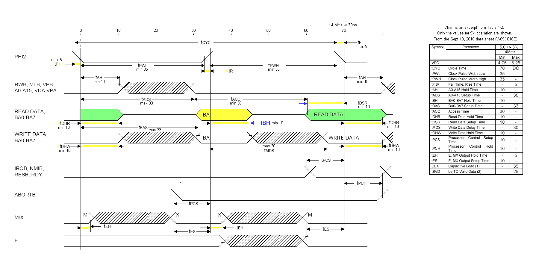
Although data to be read in is set up before the falling edge of PHI2, the description of tDHR- Read Data Hold Time- seems to imply that the read data from memory is not latched until a set hold time AFTER the PHI2 falling edge has elapsed. From what I remember about hold time: When the input data finally reaches a register's input, the register requires it's input bus to stay at the same value for a set period of time. This is so that the value can be preserved internally and propagate through to the output (possibly requiring a clock transition before the output appears), before - this is the hold time.
I therefore take the '816 timing diagram to mean that the register which receives the read data value inside the '816 might not even see the read data on it's input until after the falling edge of PHI2 has elapsed. Do I understand this correctly? My prior experience would have told me to expect that the data itself would've been latched during the falling edge itself, and the hold time would've been satisfied prior to the edge- the clock edge would just make sure the new value overwrote the old one. Since read data isn't latched on a clock edge, this must mean that internally, '816 registers are latches which don't require a clock signal to store a new value.
I apologize for the verbose explanation- but I want to actually understand this, since at one time I felt I really DID understand it all.
I've sketched out a potential dummy circuit and timing diagram (will upload later), and I still have no answer whether it's possible to do a memory-to-memory xfer in one clock cycle... just based on a preliminary sketch. Here is a verbal description of the timing:
In my sketch, as soon as VDA and VPA are low, BE is asserted, a small settling time is added* (this part I have trouble with), and then a source address is placed on the bus... source responds with data. The data is latched during the rising edge of PHI2, and the dest address is placed on the bus and data is latched into the destination on the falling edge of PHI2 (the next cycle). Immediately after the falling edge of PHI2, the DMA controller relinquishes control of the bus, gets the hell out of there, de-asserts BE, and waits till VPA and VDA are both low again.
BigEd- in another thread, Garth mentioned you do work on the Visual 6502 project... do you know how the 6502/816 is capable of delaying the assertion of bus signals. For example- in the '816, the Bank Address becomes valid just before the rising edge of PHI2. How does the '816 make sure that it loads Bank Address so far into the negative half of PHI2?
*Problem: I honestly do not remember how to add a small delay in a sequential circuit... it's been so long since I've designed hardware that I'm so used to transitions in data lines only occurring on clock edges. Going back to the delay after "BE" problem... in an ideal world, both BE assertion and the source address could occur instantaneously- i.e. the same logic circuit controls both signals- because the time required for the CPU to tristate is ideally 0 nanoseconds... but this isn't an ideal world, and so the delay is necessary.
Something else bothers me on the '816 timing that I didn't notice before:
Although data to be read in is set up before the falling edge of PHI2, the description of tDHR- Read Data Hold Time- seems to imply that the read data from memory is not latched until a set hold time AFTER the PHI2 falling edge has elapsed. From what I remember about hold time: When the input data finally reaches a register's input, the register requires it's input bus to stay at the same value for a set period of time. This is so that the value can be preserved internally and propagate through to the output (possibly requiring a clock transition before the output appears), before - this is the hold time.
I therefore take the '816 timing diagram to mean that the register which receives the read data value inside the '816 might not even see the read data on it's input until after the falling edge of PHI2 has elapsed. Do I understand this correctly? My prior experience would have told me to expect that the data itself would've been latched during the falling edge itself, and the hold time would've been satisfied prior to the edge- the clock edge would just make sure the new value overwrote the old one. Since read data isn't latched on a clock edge, this must mean that internally, '816 registers are latches which don't require a clock signal to store a new value.
I apologize for the verbose explanation- but I want to actually understand this, since at one time I felt I really DID understand it all.
Last edited by cr1901 on Sun Mar 16, 2014 4:25 am, edited 2 times in total.