6502.org Forum  Projects  Code  Documents  Tools  Forum
It is currently Sat Sep 28, 2024 11:26 pm

All times are UTC


Post new topic Reply to topic  [ 94 posts ]  Go to page Previous  1, 2, 3, 4, 5 ... 7  Next
Author Message
 Post subject: Re: First steps...
PostPosted: Sat Mar 08, 2014 3:20 am 
Offline
User avatar

Joined: Fri Aug 30, 2002 1:09 am
Posts: 8520
Location: Southern California
cr1901 wrote:
finding a female IDE connector to attach directly to the bottom of the board might be difficult

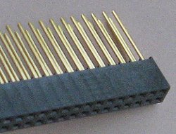
See the middle of this page of Jameco's catalog: http://www.jameco.com/Jameco/catalogs/c141/P59.pdf under ".100" (2.54mm) Female Header Receptacles".

They are available in WW too

Image

although they're pretty expensive. I got some for any customers who might want one to go with the SRAM module.

_________________
http://WilsonMinesCo.com/ lots of 6502 resources
The "second front page" is http://wilsonminesco.com/links.html .
What's an additional VIA among friends, anyhow?


Top
 Profile  
Reply with quote  
 Post subject: Re: First steps...
PostPosted: Sat Mar 08, 2014 3:52 am 
Offline
User avatar

Joined: Fri Aug 30, 2002 1:09 am
Posts: 8520
Location: Southern California
cr1901 wrote:
what happens when the drive strength of the '816 is no longer sufficient when you start adding more peripherals?

8BIT's head post at viewtopic.php?f=4&t=1908 says he was able to use my SRAM module with 8 SRAM chips on it, plus three expansion boards, plus the other stuff on the motherboard of his '816 computer, at 12MHz, with no issues. Later he said that was also without bus drivers. How much do you anticipate putting on there?

Quote:
I can't think of any conflicts offhand, but just for "preventative maintenance :P", would the addition of a bus driver on the address/data lines cause any conflicts with the process of cycle-steal DMA?

The bus driver may need to be tri-stated, depending on the configuration.

Quote:
I should probably look at the original IBM PC schematic for an example...

I haven't looked at it, but I imagine it probably has a lot of 74LS which definitely adds DC bus loading, unlike CMOS. With CMOS, you only need to total up the capacitance, and most inputs are specified to have an absolute max of 5pF, and they will usually be well under that, and a trace going to several loads will usually be less too. The '816 data sheet says they test with a 35pF load on every output. From my testing (not the data sheet), WDC's drivers seem to be approximately equal to 74AC logic which slows down by 20ps per pF of load capacitance, or 1ns for each 50pF. Not bad. It will probably be the inductance that hurts you more than capacitance, and a stronger driver won't overcome series inductance.

_________________
http://WilsonMinesCo.com/ lots of 6502 resources
The "second front page" is http://wilsonminesco.com/links.html .
What's an additional VIA among friends, anyhow?


Top
 Profile  
Reply with quote  
 Post subject: Re: First steps...
PostPosted: Sat Mar 08, 2014 5:17 am 
Offline

Joined: Wed Feb 05, 2014 7:02 pm
Posts: 158
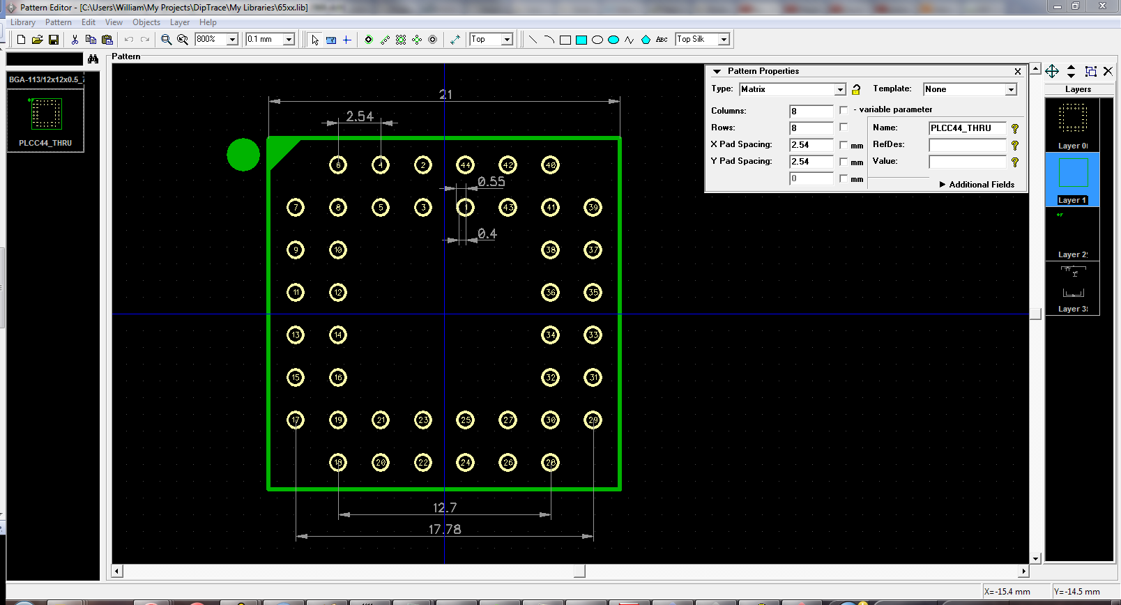
Alright, we're making progress... I've made a PLCC44 part anyway (in DipTrace), and I would like a second pair of eyes to look over the part and see whether I've made any mistakes... all units are in millimeters, and the only issue I can think of is that the PLCC socket will completely cover the solder mask (this is me being nitpicky :P)... ahh well!

DipTrace views parts from the top, and so this pattern is also viewed from the top. The measurements surrounding pad #1 are the hole and pad radii respectively.

Image

Thanks for any feedback :D! Adapting the design to a 28-pin PLCC is trivial once I've got this version down. I will submit the libraries to this forum one they're done.

P.S. Sorry about the image size... Idk how to scale it down :(.


Top
 Profile  
Reply with quote  
 Post subject: Re: First steps...
PostPosted: Sat Mar 08, 2014 8:01 am 
Offline
User avatar

Joined: Thu May 28, 2009 9:46 pm
Posts: 8404
Location: Midwestern USA
cr1901 wrote:
Alright, we're making progress... I've made a PLCC44 part anyway (in DipTrace), and I would like a second pair of eyes to look over the part and see whether I've made any mistakes... all units are in millimeters, and the only issue I can think of is that the PLCC socket will completely cover the solder mask (this is me being nitpicky :P)... ahh well!

I measured some PLCC-44 sockets I have here and came up with an average width of about 23.4mm. The official JEDEC dimension is 0.925 inches.

Your holes should have an ID of no more than 0.74mm and a pad diameter of 1.42mm, except for number 1, which should be a 1.42mm square pad with a .74mm hole. The pad diameter/size you've used leaves too little copper and will be susceptible to coming loose from the PCB when you go to solder it.

Not sure I understand your concern about the socket covering the solder mask. Unless you design otherwise, the solder mask will be covering everything except pads and via.

_________________
x86?  We ain't got no x86.  We don't NEED no stinking x86!


Last edited by BigDumbDinosaur on Sun Mar 09, 2014 7:13 pm, edited 2 times in total.

Top
 Profile  
Reply with quote  
 Post subject: Re: First steps...
PostPosted: Sat Mar 08, 2014 8:22 am 
Offline
User avatar

Joined: Thu May 28, 2009 9:46 pm
Posts: 8404
Location: Midwestern USA
cr1901 wrote:
One other thing I forgot... I was looking up whether I'd need bus drivers or not

Well, I can tell you that my POC V1.0 unit ran reliably at 12.5 MHz without the SCSI host adapter (HBA) plugged in but wouldn't boot at anything higher than 10 MHz with the HBA in place. Observation with the 'scope made it clear that the culprit was bus loading, especially the data bus, which is wired to all I/O chips, as well as the SRAM. The devices themselves don't contribute much to loading, but the traces and sockets do. Incidentally, plugging in the HBA effectively takes the buses off-board, plus adds two more sockets. That it works at 10 MHz seems to be a minor miracle. :lol:

When I did the POC V1.1 update I worked on reducing address and data bus path lengths and was able to get that unit to boot at 12.5 MHz with the HBA plugged in. However, 'scope observation still shows that the data bus is being dragged down and the edges are rounded, though not enough to cause anything to get confused. V1.1 will not boot at 14 MHz with the HBA and the data bus looks better but still shows some edge rounding and a little bit of ringing. This is with 74AC logic.

I am not going to use bus drivers in POC V2, which will use a CPLD for glue logic. I will start it off at 10 MHz and then keep bumping up the clock until it won't run. I know that the limit won't come from the CPLD, which is 10ns pin-to-pin.

Quote:
For an initial system, even with DMA, I can see the logic. However, what happens when the drive strength of the '816 is no longer sufficient when you start adding more peripherals? Will the new delay from the bus drivers cause the initial design at the original clock speed to go kaput? And would a hypothetical DMA controller need to disable the bus driver as well, or would the BE pin be sufficient?

I can't think of any conflicts offhand, but just for "preventative maintenance :P", would the addition of a bus driver on the address/data lines cause any conflicts with the process of cycle-steal DMA?

My earlier comment about being sure that everything is "downstream" of the bus drivers accounts for the skew between inputs and outputs at the drivers. You will have to use very fast logic to keep skew at a reasonable level.

During DMA, the MPU must be off the buses, which means that the bus drivers must be tri-stated. My earlier example doesn't show this, as it came from a circuit where no DMA was contemplated.

Quote:
I should probably look at the original IBM PC schematic for an example...

I suspect you'll be astonished at how much silicon (74LS) it took to get it to work.
_________________
x86?  We ain't got no x86.  We don't NEED no stinking x86!


Last edited by BigDumbDinosaur on Sun Mar 09, 2014 7:03 am, edited 1 time in total.

Top
 Profile  
Reply with quote  
 Post subject: Re: First steps...
PostPosted: Sat Mar 08, 2014 8:47 am 
Offline

Joined: Wed Feb 05, 2014 7:02 pm
Posts: 158
BigDumbDinosaur wrote:
Not sure I understand your concern about the socket covering the solder mask.
I said "solder mask", I meant "silkscreen". This is why I need to stop staying up late. In any case, I'll respond to your other points when I'm less tired.

So, some good progress today/tonight... made a dent in the pre-design tasks. Tonight, the following parts got made and laid out in DipTrace:
65816 DIP/PLCC
6521 DIP
6522 DIP
65C02 DIP (Specifically the modern CMOS variant- I assume there are no pin differences between NMOS and CMOS for other parts).
6551 DIP

Attaching the female IDE connector to the board's bottom is in fact feasible using the CAD software, contrary to what I thought.


Additionally, I started laying out the parts for my "round 1" design, to interface to an FPGA dev board... it should run close to my trial limit of 300 pins (I can increase it to 500 using a hobbyist license, which I probably will do anyway). I may need to use the onboard dev board SRAM for the time being and bootstrap using an EPROM.

EDIT: I have a better idea... Garth, are your SRAM modules in stock? How much does one cost? The SRAM module on my board could be the DMA source, initialized with dummy data during bootstrap... the dev board SRAM being the destination. The DMA controller can transfer between them and test the performance compared to the 6502 block instructions... as well as simply testing that the DMA controller works :D.

I'll leave you guys with one question tonight:
I noticed RDY is a bidirectional signal... is there a canonical way to make sure that a device and the CPU won't try to control the RDY line simultaneously?


Top
 Profile  
Reply with quote  
 Post subject: Re: First steps...
PostPosted: Sun Mar 09, 2014 7:09 am 
Offline
User avatar

Joined: Thu May 28, 2009 9:46 pm
Posts: 8404
Location: Midwestern USA
cr1901 wrote:
I noticed RDY is a bidirectional signal... is there a canonical way to make sure that a device and the CPU won't try to control the RDY line simultaneously?

The MPU will only pull RDY low if a WAI instruction is executed. So all you gotta do is connect RDY to the other device's output through a Schottky diode, with the anode connected to RDY. Be sure there is a pullup on RDY. 3.3K is a good value.

_________________
x86?  We ain't got no x86.  We don't NEED no stinking x86!


Top
 Profile  
Reply with quote  
 Post subject: Re: First steps...
PostPosted: Sun Mar 09, 2014 7:19 am 
Offline

Joined: Wed Feb 05, 2014 7:02 pm
Posts: 158
BigDumbDinosaur wrote:
cr1901 wrote:
I noticed RDY is a bidirectional signal... is there a canonical way to make sure that a device and the CPU won't try to control the RDY line simultaneously?

The MPU will only pull RDY low if a WAI instruction is executed. So all you gotta do is connect RDY to the other device's output through a Schottky diode, with the anode connected to RDY. Be sure there is a pullup on RDY. 3.3K is a good value.

But then does that arrangement allow external devices to control RDY? Is it that when the cathode of the diode is at low voltage, most voltage will be lost through the pullup, and when the cathode of the diode is at high voltage, little current flows from anode to cathode and the resistor pulls up the voltage at RDY to logic high?

This must be one of those setups where all I/O and peripherals connect to the RDY pin using pull-up resistors and any one of them can pull the line low- just like the IRQ pin.


Top
 Profile  
Reply with quote  
 Post subject: Re: First steps...
PostPosted: Sun Mar 09, 2014 7:46 am 
Offline
User avatar

Joined: Fri Aug 30, 2002 1:09 am
Posts: 8520
Location: Southern California
cr1901 wrote:
then does that arrangement allow external devices to control RDY?

They can pull it down if they're not ready to move on, as in the case of slow memory that still needs more time to get the data.

Quote:
Is it that when the cathode of the diode is at low voltage, most voltage will be lost through the pullup, and when the cathode of the diode is at high voltage, little current flows from anode to cathode and the resistor pulls up the voltage at RDY to logic high?

A Shottky diode's forward voltage drop is only around a quarter of a volt; so if the cathode is pulled nearly to ground, the anode will still be in solid "0" territory. The pull-up resistor will have about 4.4 volts on it (5V minus .25 minus I'm going with .15V at the cathode for a CMOS output that's driving 1.3mA), which will drive about 1.3mA through a 3.3K. When the cathode of the diode is higher than the anode, no current will flow through it, so the processor is not pulling RDY down against something that's trying to pull it up at the same time; ie, there's no contention. The diode will isolate them when it's biased in that direction.

_________________
http://WilsonMinesCo.com/ lots of 6502 resources
The "second front page" is http://wilsonminesco.com/links.html .
What's an additional VIA among friends, anyhow?


Top
 Profile  
Reply with quote  
 Post subject: Re: First steps...
PostPosted: Sun Mar 09, 2014 9:20 am 
Offline

Joined: Wed Feb 05, 2014 7:02 pm
Posts: 158
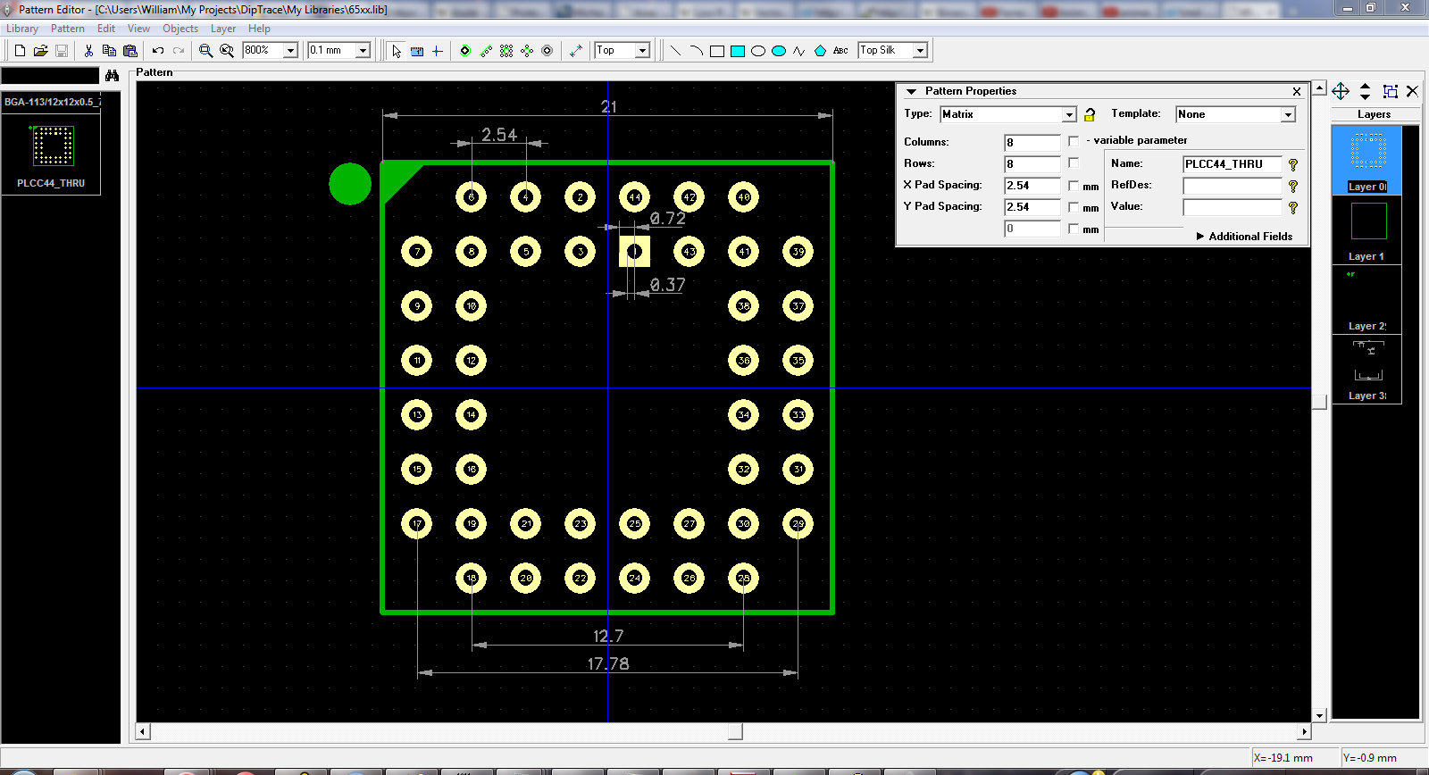
Alright, so it's how I thought the diode would work- I'm just did a poor job explaining how I thought it work.

In the meantime... is this better? Measurements are measuring the same thing as last time (the fact that pin 1's pad is a different shape is insignificant)... also, are the holes numbered correctly, looking top-down at the PCB pattern?

Image


Top
 Profile  
Reply with quote  
 Post subject: Re: First steps...
PostPosted: Sun Mar 09, 2014 6:56 pm 
Offline
User avatar

Joined: Thu May 28, 2009 9:46 pm
Posts: 8404
Location: Midwestern USA
cr1901 wrote:
But then does that arrangement allow external devices to control RDY? Is it that when the cathode of the diode is at low voltage, most voltage will be lost through the pullup, and when the cathode of the diode is at high voltage, little current flows from anode to cathode and the resistor pulls up the voltage at RDY to logic high?

This must be one of those setups where all I/O and peripherals connect to the RDY pin using pull-up resistors and any one of them can pull the line low- just like the IRQ pin.

See following.
Attachment:
File comment: Driving RDY From Other Logic
rdy_ckt.gif
rdy_ckt.gif [ 25.45 KiB | Viewed 1053 times ]
Unless both inputs on the NAND gate are high, the output of the gate will be high and RDY will not be affected in any way. If the MPU executes WAI during this time, the diode will be reverse biased and RDY will go low. If both NAND inputs go high, the gate's output will go low and pull RDY low, regardless of what the MPU is doing. That's all there is to it.

As Garth noted above, the worst-case current flow will be about 1.4 MA through the 3.3K resistor, so size the diode accordingly.

_________________
x86?  We ain't got no x86.  We don't NEED no stinking x86!


Top
 Profile  
Reply with quote  
 Post subject: Re: First steps...
PostPosted: Sun Mar 09, 2014 7:07 pm 
Offline
User avatar

Joined: Thu Dec 11, 2008 1:28 pm
Posts: 10938
Location: England
Would it not be appropriate to use a logic gate with an open-collector output?


Top
 Profile  
Reply with quote  
 Post subject: Re: First steps...
PostPosted: Sun Mar 09, 2014 7:10 pm 
Offline
User avatar

Joined: Thu May 28, 2009 9:46 pm
Posts: 8404
Location: Midwestern USA
cr1901 wrote:
In the meantime... is this better? Measurements are measuring the same thing as last time (the fact that pin 1's pad is a different shape is insignificant)... also, are the holes numbered correctly, looking top-down at the PCB pattern?

The pad and hole sizes look to be okay. The square pad denoting pin 1 is useful during the "wiring up" phase of PCB layout.

The 21mm width and height of the socket body is incorrect. The JEDEC standard for a PLCC-44 through-hole socket is 0.925 inches or 23.48mm. Take a look at this drawing for socket details.

Incidentally, in PCB production, hole and pad sizes are expressed in diameter, not radius.

_________________
x86?  We ain't got no x86.  We don't NEED no stinking x86!


Top
 Profile  
Reply with quote  
 Post subject: Re: First steps...
PostPosted: Sun Mar 09, 2014 7:25 pm 
Offline
User avatar

Joined: Thu May 28, 2009 9:46 pm
Posts: 8404
Location: Midwestern USA
BigEd wrote:
Would it not be appropriate to use a logic gate with an open-collector output?

Sure, if one is available for the application. It would be easy in a PLD to tri-state the output when not wait-stating.

However, if the wait-state circuit is being implemented in discrete logic, it may be that RDY will be driven from the Q output of a flip-flop. So the diode would become de rigueur.

_________________
x86?  We ain't got no x86.  We don't NEED no stinking x86!


Top
 Profile  
Reply with quote  
 Post subject: Re: First steps...
PostPosted: Wed Mar 12, 2014 11:22 am 
Offline

Joined: Wed Feb 05, 2014 7:02 pm
Posts: 158
Provided I got a second/third pair of eyes to look over my schematic, would it be an exceptionally bad idea to just get the PCB made (two layer) and skip the wire-wrap portion? I could always make corrections to a two-layer PCB, and money's a bit tight for wire wrap parts.

Right now, I'm just using CAD software to develop the schematic- it could always be used as a guide to develop the wire-wrap circuit as well.


Top
 Profile  
Reply with quote  
Display posts from previous:  Sort by  
Post new topic Reply to topic  [ 94 posts ]  Go to page Previous  1, 2, 3, 4, 5 ... 7  Next

All times are UTC


Who is online

Users browsing this forum: No registered users and 13 guests


You cannot post new topics in this forum
You cannot reply to topics in this forum
You cannot edit your posts in this forum
You cannot delete your posts in this forum
You cannot post attachments in this forum

Search for:
Jump to: