6502.org Forum  Projects  Code  Documents  Tools  Forum
It is currently Sat May 04, 2024 8:18 pm

All times are UTC


Post new topic Reply to topic  [ 37 posts ]  Go to page Previous  1, 2, 3  Next
Author Message
PostPosted: Fri Feb 21, 2014 12:45 pm 
Online
User avatar

Joined: Thu Dec 11, 2008 1:28 pm
Posts: 10797
Location: England
On the point that zp-I/O devices will need to be fully decoded, note that on-chip decoding is pretty cheap. That's why the 6510 and WDC's SoC offerings can do it. An FPGA 6502 could also do on-chip decoding - either with the I/O devices also on-chip, or by outputting some useful decoded signals, such as 'zp' or even 'bottom 16 bytes of zp' or indeed even a specific chip-select.

A design which uses a CPLD to deal with the address bus could also output a fully decoded chip select, or a partially decoded signal.

Cheers
Ed


Top
 Profile  
Reply with quote  
PostPosted: Fri Feb 21, 2014 5:26 pm 
Offline
User avatar

Joined: Fri Dec 11, 2009 3:50 pm
Posts: 3351
Location: Ontario, Canada
BigEd wrote:
An FPGA 6502 could also do on-chip decoding - either with the I/O devices also on-chip, or by outputting some useful decoded signals
I like that idea. But by far the biggest gain comes from the BBSn/BBRn and SMBn/RMBn instructions, and we don't have a 6502 core that offers those -- yet. No doubt they could be added to an existing core. (Another project for your list, Ed? :wink: )
GARTHWILSON wrote:
Using your single-cycle output port [...] takes it down to 121 cycles
That single-cycle output port sure speeds things up, alright. And it could accelerate inputting the MISO signal, too (although not as dramatically).

By adding an AND (or NAND) gate as shown, the code to input the MISO signal speeds up due to elimination of the "BIT VIA3PB" instruction -- or whatever you're presently using. You'd need to execute CLV after a "1" is received, but it's still faster. (If you're not presently able to use BIT, then you'll have some much-slower alternative -- and greater potential for speedup.)


Attachments:
Ultra-fast_65c02_SPI_IO.gif
Ultra-fast_65c02_SPI_IO.gif [ 5.91 KiB | Viewed 1230 times ]

_________________
In 1988 my 65C02 got six new registers and 44 new full-speed instructions!
https://laughtonelectronics.com/Arcana/ ... mmary.html
Top
 Profile  
Reply with quote  
PostPosted: Fri Feb 21, 2014 7:01 pm 
Offline
User avatar

Joined: Mon Apr 23, 2012 12:28 am
Posts: 760
Location: Huntsville, AL
At least the following:
(1) M65C02 on GitHUB or M65C02 on OpenCores
(2) cpu65c02_true_cycle on OpenCores

_________________
Michael A.


Top
 Profile  
Reply with quote  
PostPosted: Fri Feb 21, 2014 7:18 pm 
Offline
User avatar

Joined: Fri Dec 11, 2009 3:50 pm
Posts: 3351
Location: Ontario, Canada
Excellent, Michael! Evidently I was fixating on Arlet's core. Thanks for correcting me.

_________________
In 1988 my 65C02 got six new registers and 44 new full-speed instructions!
https://laughtonelectronics.com/Arcana/ ... mmary.html


Top
 Profile  
Reply with quote  
PostPosted: Fri Feb 21, 2014 7:24 pm 
Offline
User avatar

Joined: Fri Aug 30, 2002 1:09 am
Posts: 8431
Location: Southern California
That's the first time I've ever seen what I consider to be a truly legitimate use of SO\, due to connecting it to the single-cycle output port with a NAND to help control when the edge is accepted.

The fine-grained onboard address decoding in the 65134 and '265 seem to cut its speed in half compared to the 'c02 and '816.  Admittedly other microcontrollers are reaching far greater clock speeds in spite of their fine-grained onboard address decoding, and I don't know if it's just a different wafer process or if it's because of greater pipelining.  [Edit:  Three years later, Bill Mensch told me the '134 and '265 may indeed go a lot faster than specified, but they just haven't tested them to that.]

_________________
http://WilsonMinesCo.com/ lots of 6502 resources
The "second front page" is http://wilsonminesco.com/links.html .
What's an additional VIA among friends, anyhow?


Top
 Profile  
Reply with quote  
PostPosted: Fri Feb 21, 2014 7:33 pm 
Online
User avatar

Joined: Thu Dec 11, 2008 1:28 pm
Posts: 10797
Location: England
(Those chips may run slower but I can't see that we know enough to blame the on-chip address decoding. For the 16-bit PC to increment in a clock cycle, it's necessary to detect &7FFF - that's a 15-input gate, in effect. In practice it isn't a 15-input gate, but hopefully you see the point.)


Top
 Profile  
Reply with quote  
PostPosted: Fri Feb 21, 2014 7:43 pm 
Offline
User avatar

Joined: Fri Dec 11, 2009 3:50 pm
Posts: 3351
Location: Ontario, Canada
BigEd wrote:
Those chips may run slower but I can't see that we know enough to blame the on-chip address decoding.
I had that thought, too. And there's an on-chip ROM, correct? Could that limit the speed? (I'm just guessing, based on what the microcontroller has that the microprocessor doesn't.) In support of Garth's theory, though, the I/O decode has less than 1/2 a clock cycle to become valid. I know the PC increment was just for comparison, but the timing requirement in that case may be a lot less stringent.

GARTHWILSON wrote:
That's the first time I've ever seen what I consider to be a truly legitimate use of SO\, due to connecting it to the single-cycle output port with a NAND to help control when the edge is accepted.
Glad you like it, but surely there are other legitimate examples?? Wasn't /SO used on a Commodore disk drive or something like that? In any case, you'd have to control when the edge is accepted... unless you're willing to entirely forego normal use of the Overflow flag. (Maybe there's no call for signed arithmetic in a Commodore disk drive!)

_________________
In 1988 my 65C02 got six new registers and 44 new full-speed instructions!
https://laughtonelectronics.com/Arcana/ ... mmary.html


Top
 Profile  
Reply with quote  
PostPosted: Fri Feb 21, 2014 8:43 pm 
Offline
User avatar

Joined: Thu May 28, 2009 9:46 pm
Posts: 8173
Location: Midwestern USA
Dr Jefyll wrote:
Wasn't /SO used on a Commodore disk drive or something like that? In any case, you'd have to control when the edge is accepted... unless you're willing to entirely forego normal use of the Overflow flag. (Maybe there's no call for signed arithmetic in a Commodore disk drive!)

It was use in the 1540 and 1541 drives to produce rapid response when the disk was ready with/for data. Dunno about the IEEE models though.

I used SOB (that's what WDC calls it) in a 65C02 SBC about 22 years ago for my DREQ (DMA request) connection with an NCR 53C90A SCSI controller, the ancestor of the 54C94 I'm using in POC. A BVC to itself watched for a transition and then the read or write access occurred, followed by CLV and a return to the BVC loop. Wish I could do that with the 65C816.

_________________
x86?  We ain't got no x86.  We don't NEED no stinking x86!


Top
 Profile  
Reply with quote  
PostPosted: Fri Feb 21, 2014 8:48 pm 
Online
User avatar

Joined: Thu Dec 11, 2008 1:28 pm
Posts: 10797
Location: England
As an aside, about the SO pin, formerly known as CPS (for Chuck Peddle Special)...
BigDumbDinosaur wrote:
I used SOB (that's what WDC calls it)

Before WDC, there was MOS, and:
Quote:
The group was not without humour. One of the important designers on this chip was Rod Orgill (who can be seen in this picture). Bill said that one of the 6502 pins is officially named SO (Set Overflow). “Chuck, Rod, and I know that it’s real name is Sam Orgill… Rods dog”.

(from http://www.commodore.ca/commodore-histo ... -the-6502/)


Top
 Profile  
Reply with quote  
PostPosted: Fri Feb 21, 2014 10:00 pm 
Offline
User avatar

Joined: Fri Dec 11, 2009 3:50 pm
Posts: 3351
Location: Ontario, Canada
BigDumbDinosaur wrote:
I used SOB (that's what WDC calls it) in a 65C02 SBC about 22 years ago [...] A BVC to itself watched for a transition and then the read or write access occurred, followed by CLV and a return to the BVC loop.
Cool! As to the point about unwanted transitions interfering with normal use of the Overlow flag, is there a hardware gate used or is the problem avoided just by the fact the peripheral chip won't generate that signal until issued a command to do so? And is it the same for the 1540 and 1541?

_________________
In 1988 my 65C02 got six new registers and 44 new full-speed instructions!
https://laughtonelectronics.com/Arcana/ ... mmary.html


Top
 Profile  
Reply with quote  
PostPosted: Sat Feb 22, 2014 2:55 am 
Offline
User avatar

Joined: Thu May 28, 2009 9:46 pm
Posts: 8173
Location: Midwestern USA
Dr Jefyll wrote:
BigDumbDinosaur wrote:
I used SOB (that's what WDC calls it) in a 65C02 SBC about 22 years ago [...] A BVC to itself watched for a transition and then the read or write access occurred, followed by CLV and a return to the BVC loop.
Cool! As to the point about unwanted transitions interfering with normal use of the Overlow flag, is there a hardware gate used or is the problem avoided just by the fact the peripheral chip won't generate that signal until issued a command to do so? And is it the same for the 1540 and 1541?

I no longer recall the details of what was going on in the 154x drives, but can say that in the driver code that ran the SCSI interface in my long-ago SBC project, there was nothing that would have accidentally set the V bit. The 53C90 would not affect SOB unless the former's 16 bit transfer counter was loaded with a non-zero value and a DMA instruction was issued. Once that instruction was issued, the 'C90 would assert DREQ as soon as it had or was ready for a byte. DREQ was connected to SOB through an inverter. After the read or write instruction had been executed on the 'C90, DREQ would de-assert until the 'C90 had more or was ready for more. When the 16 bit transfer counter reached zero, DREQ went high-Z. This basic principle is used in POC's host adapter, minus the SOB connection.

_________________
x86?  We ain't got no x86.  We don't NEED no stinking x86!


Top
 Profile  
Reply with quote  
PostPosted: Sat Mar 01, 2014 10:58 am 
Offline
User avatar

Joined: Fri Dec 11, 2009 3:50 pm
Posts: 3351
Location: Ontario, Canada
Earlier in this thread...
GARTHWILSON wrote:
full address decoding [...] would reduce the maximum clock speed, unless I resorted to programmable logic.

One way to preserve maximum clock speed, even without programmable logic, is to wait-state the I/O. The resultant performance trade-off can be minimized, as explained later.

In the case of a 'C02 system that's lacking programmable logic, clocked at maximum speed, and using the wait-state solution, I/O in zero-page is still a clear win. An '816 system subject to all the same restrictions will have no benefit performance-wise; however, it and the 'C02 both save program memory by using zero-page/direct-page addressing mode.

Further improvement occurs if any of the restrictions are relaxed (slower clock, and/or programmable logic is available), because wait states become unnecessary. A 'C02 system will get 100% of the benefit of I/O in zero-page. Unfortunately the '816 doesn't have SMB RMB BBS and BBR instructions, but (like the 'C02) it will save one cycle and one byte for each occurrence of LDA STA BIT TSB TRB etc with zero-page/direct-page addressing.

Attachment:
zero-page decoder and wait-state generator.gif
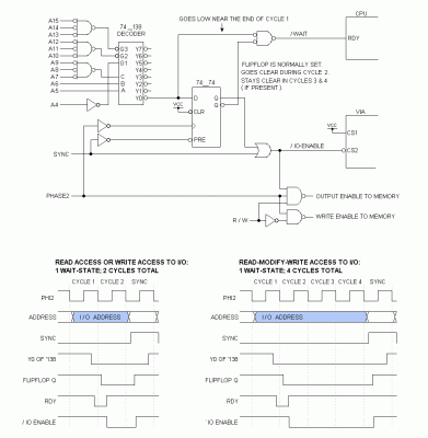
zero-page decoder and wait-state generator.gif [ 18.04 KiB | Viewed 1200 times ]

The circuit above includes wait state logic and full decoding for a 6522 VIA mapped into zero page. Read-Modify-Write instructions incur only one wait state, not three. This preserves the substantial performance advantage offered by SMB and RMB -- instructions custom tailored for fast I/O! The more general R-M-W instructions such as INC DEC TSB and TRB also incur only one wait state, as do simple reads and writes such as BIT LDA STA AND ORA etc.

If I were building this I'd use 74LVC1G332's for the three 3-input OR gates at the top left. These guys come in a painfully tiny 6-pin DIP but boast 3-ns maximum propagation delay. The 74_138 decoder is available in a long list of high-speed families, including 74AC and 74BCT.

In the timing diagrams, cycle one is the wait state, when the zero-page address first appears. Because no data is transfered in cycle 1, we're freed from the usual stipulation that the VIA CS must be asserted before Phase 2 begins. Instead it's sufficient merely to bring the CPU RDY input low tPCS before Phase 2 ends.

Memory is not yet inhibited, so an unused memory access occurs in cycle one. Since RDY gets pulled low in cycle 1, cycle 2 is the same address all over again -- but this time accessing the VIA instead of memory. In cycle 2 there's no difficulty getting the VIA chip-select asserted before Phase 2 begins, because tADS (the CPU address delay) and the decoder propagation delay have already elapsed -- those signals are stable.

Next we have either the beginning of the next instruction (marked by SYNC), or cycles 3 & 4 and then the beginning of the next instruction (marked by SYNC). :) It's actually the SYNC signal that ends the VIA chip-select -- and here again we avoid the decoder propagation delay. The SYNC signal is passed to the VIA with just a single gate-delay (the 2-input OR). It's always this same path that ends the VIA chip select, regardless of whether the access is read-modify-write or just a simple read or write. That's why the two timing diagrams end with the identical sequence.

-- Jeff

_________________
In 1988 my 65C02 got six new registers and 44 new full-speed instructions!
https://laughtonelectronics.com/Arcana/ ... mmary.html


Last edited by Dr Jefyll on Wed Jun 11, 2014 4:01 am, edited 1 time in total.

Top
 Profile  
Reply with quote  
PostPosted: Sat Mar 01, 2014 5:19 pm 
Offline
User avatar

Joined: Sun Jun 30, 2013 10:26 pm
Posts: 1928
Location: Sacramento, CA, USA
I am not personally qualified to comment on the feasibility of your design, but I somehow feel the need to congratulate you for such a well-polished and attractive post, doc!

Mike


Top
 Profile  
Reply with quote  
PostPosted: Sat Mar 01, 2014 7:57 pm 
Offline
User avatar

Joined: Fri Dec 11, 2009 3:50 pm
Posts: 3351
Location: Ontario, Canada
Thanks, Mike. I'm glad you find that post attractive, 'cause this one is gonna make ya wanna retch!
Attachment:
DBV IC package.gif
DBV IC package.gif [ 325.81 KiB | Viewed 1184 times ]
Did I mention that the 74LVC1G332 comes in a painfully tiny package? Actually you have three options to choose from: painfully tiny, agonizingly tiny, and just stupifyingly small. I'd recommend the comparatively gargantuan DBV package, shown here to scale on a .1" grid of plate-through holes. Some people would find these excessively small for proto-board hacking, but I'm too stubborn to admit defeat, so here's how I'd deal with these puppies. (Really you want a PCB for these if you can manage it.)

In the arrangement at the top left we have the benefit of soldering four pins to the board, with the remaining two pins (2 & 5) requiring flying leads. Unfortunately those two are the power supply, and deserve the best connections. The other arrangement uses four flying leads, but the power pins can have solid connections (and possibly a SMD bypass cap) directly on the opposite side. Putting a little bend in the other four pins will ensure they don't contact anything they shouldn't, and wirewrap wire is a workable gauge for the flying leads.

Needless to say, pairing some 74LVC1G332's with a '138 is just one of many ways to decode a zero-page address. But the 3ns prop delay makes 74LVC1G332's very attractive.

-- Jeff

_________________
In 1988 my 65C02 got six new registers and 44 new full-speed instructions!
https://laughtonelectronics.com/Arcana/ ... mmary.html


Top
 Profile  
Reply with quote  
PostPosted: Sun Mar 02, 2014 12:54 am 
Offline
User avatar

Joined: Sun Jun 30, 2013 10:26 pm
Posts: 1928
Location: Sacramento, CA, USA
How about one of these little guys, Jeff?

Attachment:
sot363.JPG
sot363.JPG [ 53.23 KiB | Viewed 1172 times ]


Mike


Top
 Profile  
Reply with quote  
Display posts from previous:  Sort by  
Post new topic Reply to topic  [ 37 posts ]  Go to page Previous  1, 2, 3  Next

All times are UTC


Who is online

Users browsing this forum: BigEd and 10 guests


You cannot post new topics in this forum
You cannot reply to topics in this forum
You cannot edit your posts in this forum
You cannot delete your posts in this forum
You cannot post attachments in this forum

Search for:
Jump to: