6502.org Forum  Projects  Code  Documents  Tools  Forum
It is currently Tue Sep 24, 2024 11:18 am

All times are UTC


Post new topic Reply to topic  [ 5 posts ] 
Author Message
PostPosted: Tue Oct 22, 2013 9:06 am 
Offline

Joined: Tue Oct 22, 2013 8:50 am
Posts: 6
I have read a bit on how the 6502 processes instructions but im still a bit confused. From a diagram of a normal pla there is an input with a normal line and an inversion of that same line, and there are lines of the array attached to nothing, then those lines lead to the nor section which go down into the output. Image

What is the purpose of the inputs and the outputs? I saw that it fires instructions based on timing, but I don't know where that goes in on that schematic. Im attempting to better understand processors and this is a bit confusing to me. I've looked at simulations and i've come up with what I THINK is going on but this might be something different.

So there might be triggers for parts of the cpu, like (Accumulator INPUT) (Accumulator OUTPUT) (X input) (X output) (Load) (Store) etc etc..

And STA might trigger Store, and A, which will select A to dump it's data into the register bus, where the store circuit will pick that up and send it to whatever address is in the argument registers. (example, STA $0D00) would trigger Store, and A. LDA will trigger Load and A, which will pull the data from the address in the argument registers into the register bus and only A will pick that up and lock on the next clock cycle.

I'm aiming to build a very simplified processor from relays or transistors as a project. Instead of being 8 bit it will be 4 bit, the addresses will be 1 byte, which will give me enough room to do very basic functions, allow 16 different instructions. From there i might expand but all in all I'm just trying to learn. Thanks for your help.


Top
 Profile  
Reply with quote  
PostPosted: Tue Oct 22, 2013 12:47 pm 
Offline
User avatar

Joined: Mon Apr 23, 2012 12:28 am
Posts: 760
Location: Huntsville, AL
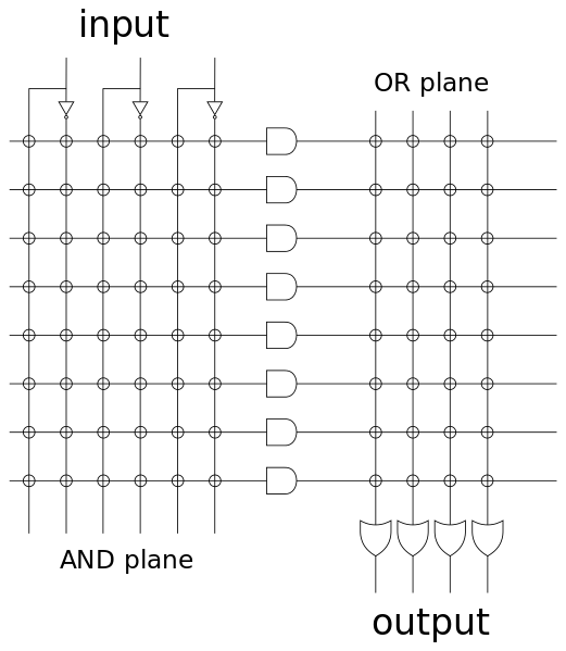
In the most simplistic terms, the Programmable Logic Array (PLA) is a device that allows logic products to be summed (combined) to form a logic signal. The logic products are represented by the AND terms, and the sums are represented by the OR terms.

In your diagram, the inputs are put into the device as true and not true terms. Another array wires crossing under these input wires collect these terms into a single product. As represented in your diagram, the product term can consist of any of the inputs and their complements.

A second array of wires allows the product terms to be collected into sums of product terms. Thus, the output each of the AND gates functions as an input to this second array, and another set of wires below them allow these terms to be collected into sums of products which are the outputs of the ORs shown on your diagram.

In the 6502 and similar processors which use PLAs, the IR (instruction register), the processor sequencer, and other signals such as the processor flags are provided as inputs to the PLA. The number of OR terms is generally much higher than the number of inputs so that their outputs can be used to control specific logic circuits.

In the 6502, the IR is an 8-bit register, the processor sequencer must represent at least 7 memory cycles (so it's at least 3 bits in width), IRQ, NMI, the ALU flags (NVZC), Interrupt Mask (I), Decimal Mode Flag (D), memory ready (RDY), etc., are inputs to the PLA.

Elsewhere on the Internet there's a block diagram of the 6502 (Hanson's Block Diagram) that shows that the number of inputs signals into the PLA are 21 and the number of outputs are 130. This means that there are at least 42 (true and not true) inputs into the first array of your diagram, and that there are 130 OR gates collecting product terms in the second array of your diagram. However, there's no direct way to determine the number of AND gates used to develop the product terms collected by the OR gates.

The beauty of a logic arrays like the one used in the 6502 is its ability to be tailored specifically to the requirements of the application. As a user programmable element, there's a practical limit imposed by the process used in its implementation. Thus, PLAs tend to have a fixed number of AND terms and a fixed number of OR terms. The 6502 uses a logic array where the number of AND and OR terms is determined by the designer.

As you can also see in the referenced block diagram, there's feedback from the decode logic into the processor sequencer. This feedback determines the next cycle of the sequencer. Because the designer used a PLA in the implementation, at each state in the sequencer, the designer is able to take a branch to the appropriate next state with a minimal amount of logic. Further, the state transitions equations have access to the current state of all critical signals and the instruction register. Together, the decode logic and the sequencer can minimize the number of distinct states required to implement the complex addressing modes of the 6502.

Viewed as a Finite State Machine (FSM), the 6502 is best characterized as a Mealy model FSM. Without the regularity provided by the PLA, the implementation of the 6502 would have been significantly more difficult in "random" logic.

That being said, there's a penalty to be paid by using a PLA: PLAs are generally slower than random logic. But I'm of the opinion that given the technology of the time, the lower operating speed imposed by the PLA was compensated for by the improved efficiency of the processor as whole. This is supported by claims made by others on this forum and elsewhere regarding the performance of a 6502 at 1MHz compared to the performance of an 8080 at 4MHz.
Attachment:
File comment: 6502 Block Diagram - Hanson
6502-BlockDiagram-Hanson.jpg
6502-BlockDiagram-Hanson.jpg [ 1.61 MiB | Viewed 2342 times ]

_________________
Michael A.


Top
 Profile  
Reply with quote  
PostPosted: Tue Oct 22, 2013 3:13 pm 
Offline

Joined: Tue Oct 22, 2013 8:50 am
Posts: 6
What I'm understanding is that the PLA is an easier way to decode a signal into a broken up set of selectors for the function components that the instruction calls for depending on the timing.. so if the opcode for LDA zeropage is A5, that will break down into selecting different parts at different times, maybe it will take the operand from the operand registers and put it in the address low byte register, in the next timing it might call that address and put the resulting data in that location into a register, in the next timing it might open A for input, in the next timing it might dump that data in the register bus which only A is open to, the next timing might close A from the register bus, and the next timing might be to increment the program counter according to how many bytes that instruction takes, and then it will load another instruction and do the same thing in a possibly different order selecting diferent things at different times. I'm not quite sure yet but i'm hoping to learn more. Your explanation was very helpful though.. thank you. I hope to get further into this. :)


Top
 Profile  
Reply with quote  
PostPosted: Tue Oct 22, 2013 4:45 pm 
Offline
User avatar

Joined: Mon Apr 23, 2012 12:28 am
Posts: 760
Location: Huntsville, AL
Too many states in your description, but essentially correct. You should be able to perform the operations required by the instructions in at least the same number of cycles as required by the current 6502:

(1) Fetch opcode, increment PC;
(2) fetch zeropage address operand, increment PC;
(3) fetch zeropage data, write into A;
(4) fetch opcode, increment PC;
(5) etc.

Or

(1) Fetch opcode, increment PC;
(2) fetch zeropage address operand, increment PC;
(3) fetch zeropage data, latch input data;
(4) transfer input data latch into A, fetch opcode, increment PC;
(5) etc.

The two phase nature of the 6502 cycle can be taken advantage of so that when Phi1 is high certain micro-operations take place, and then when Phi2 is high another set of micro-operations take place.

_________________
Michael A.


Top
 Profile  
Reply with quote  
PostPosted: Tue Oct 22, 2013 5:42 pm 
Offline
User avatar

Joined: Thu Dec 11, 2008 1:28 pm
Posts: 10938
Location: England
Hi
Just a couple of points to add:
- A PLA is just an implementation tactic, for constructing complex logical combinations of inputs to produce some outputs. It's compact, and it's regular, which makes it good for chips. But it is just a bunch of logic gates.
- The 6502's instruction decoder is not really a PLA or a ROM. It's more like half a PLA - the input half. In NMOS chips, you find that NOR gates are strongly preferred compared to NAND gates, and indeed the PLA is a compact and regular way to construct 130 or so NOR gates whose inputs come from the Instruction Register and the Timing Generator. The outputs of these go into the "random logic" which is an unstructured collection of many more gates - mostly NOR-style but also complex gates. The outputs of those do become the control signals for the datapath and for various latches and muxes around the chip. (The 6502 is not a regular design - it's hacked down to be compact and efficient.)

Cheers
Ed


Top
 Profile  
Reply with quote  
Display posts from previous:  Sort by  
Post new topic Reply to topic  [ 5 posts ] 

All times are UTC


Who is online

Users browsing this forum: No registered users and 107 guests


You cannot post new topics in this forum
You cannot reply to topics in this forum
You cannot edit your posts in this forum
You cannot delete your posts in this forum
You cannot post attachments in this forum

Search for:
Jump to: