Note: this top post will be updated as neededCurrent version: CHOCHI H.
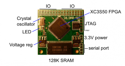
Assembled boards available. PM me...Summary: CHOCHI is a minimal XC3S50 FPGA board with 128K of fast SRAM and 31 IO pins, capable of hosting Arlet's 6502 core with up to 128K RAM with about 1/2 the resources available for custom circuitry. It is closely related to DILDAR50
http://forum.6502.org/viewtopic.php?f=10&t=2638- in fact the upper IO connector is identical in later boards. Final prototypes of CHOCHI even carry the DILDAR insignia.:
Attachment:
 Introducing.png [ 104.63 KiB | Viewed 17396 times ]
For more information also visit
http://apple2.x10.mx/CHOCHIMotivationCHOCHI was driven by the desire for a minimal, inexpensive 6502 controller that is more capable than DILDAR50 (more than 8K of RAM). CHOCHI, in its minimalism, matches the spirit as well as the requirements for retrocomputing. It is big enough to fit a full 6502 system (including serial, parallel, and in the future, SD card and video interfaces). Working with it requires a minimal mindset that we are familiar with and the rest of the world finds absurd. And it helps that it is inexpensive enough to be nearly disposable.
Minimal RequirementsThe board requires a regulated 3.3V power supply, and a 115,200 serial port connection to your PC. A terminal program capable of sending binary files directly is also needed (I use gtkterm on linux).
Skill levelTo use this board you need to be reasonably comfortable hooking up and configuring a serial port on your computer, be able to compile or assemble 6502 code. Minimal soldering skills are required to connect to IO ports. Advanced users may reconfigure the FPGA to fine-tune the system to their liking, or do something completely different.
AvailabilityAs an experiment I am happy to offer members of 6502.org assembled boards for about $35. PM me if you are interested. Open source access to all Verilog and design files (gEDA PCB); all files CHOCHI files created by me should be considered as public domain if your country accepts it, or a compatible open license of your choosing.
Design notesCHOCHI started its life as DILDAR50. The bottom IO connector was removed and IO recycled to connect the SRAM. Two remaining pins were used as a dedicated serial connector (lower right). Unlike DILDAR, the power regulators are right on top. There are no parts on the bottom, making it much easier to manufacture. The board can actually accomodate a 512K SRAM.
Initial configurationThe board comes pre-configured with a 45MHz 6502 core (Arlet's) with almost 64K RAM (and some IO). The system boots into a loader on power-up. The initial configuration features
-LED output ($C000, also top left pin)
-UART ($C008, special pins, 115200 baud, no parity, 2 stop bits works best)
-8-bit output port ($C010, top row right side)
-8-bit input port ($C018, bottom row, right side)
-Reset button port(2nd top pin from left)
Memory MapCode:
$0000-$01FF BRAM
$0200-$BFFF SRAM
$C000-$C0FF IO
$F800-$F9FF Mapped to $0000-$01FF
$FA00-$FFFF BRAM, upon bootup contains loader and vectors
6502 softwareLink to FIG-FORTH post:
http://forum.6502.org/viewtopic.php?f=10&t=2644&p=28311#p28311The loader accepts a binary file prefixed by 16-bit address and 16-bit size. So far I managed to get Daryl's monitor, Fig-Forth and EhBASIC running, with a little help from my friends here. Thank you.


