I have not shopped for can oscillators in years, but I remember them being pretty power-hungry. One 65c02 design I did for a commercial product usually took less than 2mA for the entire computer.
The thriftiest ones I found were 1 MHz, half-size, about 4 mA, which is one third of the entire computer's power consumption... another third went on a diode-based logic gate

- No speeds over the "classic" ones (up to 19200 kb/s) are needed
You can go at least six times that fast-- just not with the 1.8432MHz crystal being used to get the baud rate.
<snip>
The bit rate will be 1/16 of the RxC input clock.
But then you lose the flexibility of software-selected baud rate, unless some extra circuitry is added... incidentally, the 115200 kb/s usual on "modern" PCs is exactly 1/16 of 1.8432 MHz.
I've also used it without RTS & CTS, in situations where there was no danger of overruns.
At the more-or-less standard speed of 9600 b/s, one character takes roughly 1 ms to transmit. If there's a human being typing on a keyboard what is transmitted, you'll surely do well without RTC/CTS... and even without FIFO!
IIRC, MS-DOS recommended not disabling interrupts for longer than 1 ms, which fits well the above scenary.
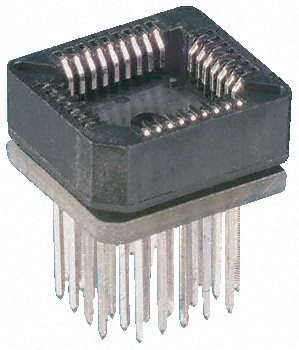
However, I think those pins are like the pin-header ones, of square section... it seems they won't fit a breadboard (at least, not mine)
- Pedantic computer science note:
 the data structures you would use with a UART are actually FIFOs, not buffers. I know: picky, picky.
Pedantic notes are welcome and encouraged FIFO is certainly the name I chose for the corresponding kernel functions...
You can isolate the output of the 'AC74 flop (not 'HC74—probably not fast enough for a 10 MHz system in which wait-states are to be implemented) from RDY with a Schottky diode
<snip>
Better that the 4.7K resistor be 3.3K (it's required due to the diode). Also, the connection from the diode to RDY should be as short and direct as possible.
I'm not fond of diodes on digital lines  I designed an OR logic gate around a couple of diodes plus a 1 K resistor (trying to get it as fast as possible), everything tightly connected... it drew of course "a lot" of power (4 mA), but high-to-low transitions (this was OR with pull-down resistor, the opposite you mention) were painfully slow: a whopping 100 nS
  And I think RDY would be much more sensitive to a sluggish low-to-high transition (when a pull-up resistor is used) than, say, IRQ\ – which has quite a few cycles to settle.
Anyway... my current 65C02's in DIP-40 are GTE and Rockwell, thus no WAI instruction 
I don't want to rain on your parade, but it's unlikely that you could implement the required logic using discrete devices and achieve sufficiently fast operation to actually stop a memory or I/O access from occurring.
The key here is that I won't prevent illegal accesses, but only illegal writes. Since such operations are qualified (typically by ø2), I've got some time for it  I'm aware that some reads to peripheral devices may be dengerous (like clearing interrupts, etc) but they're usually harmless...
Can't tell for sure because I haven't build this circuit yet, but... a picture is worth a thousand words:
 Viewed 779 times")
- Illegal instruction/access protection circuit for 6502
The only specific signals here are:
- KERNEL\ is active (low) when the current address is in kernel space -- can't really talk about user/supervisor modes on a 6502. Instructions fetched when this signal is active, have no restrictions at all.
- PROT\ is active (low) when the current address is in protected space -- maybe I/O devices, system variables of whatever zone must be protected from direct user alterations.
Both signals may be easily derived from the address decoding logic. This circuit
generates two internal signals (
SEI\ and
WD\, more on them later) but the rest is regular 6502 stuff.
First of all, for each fetched instruction it's decided whether it has full privileges or not -- by latching the state of
KERNEL\. Clocking the flip-flop by SYNC alone
won't work, because this one changes more-or-less at the same time as the address lines, and KERNEL\ derives from these --
after the delay from decoding logic. Thus, SYNC is gated thru ø2, when all addresses and decoding are expected to be stable.
Whenever an instruction
in user space is fetched, the
protection devices get enabled... for the illegal instructions, it may be as simple as a '688 comparator: one side of it goes to the data bus, the other is hardwired to the desired "illegal" opcode -- for instance, $78 for
SEI, which would ruin
preemptive multi-tasking if accidentally executed. However, as soon as this comparator is enabled, data
may not be correct: that's only guaranteed
a bit before the end of the cycle. That's why I put another flip-flop at the comparator's output, getting updated by ø1 -- in other words, when ø2 goes down; data will be hold
a slight time after that, more with propagation delays.
The "problem" with this second FF, is that the NMI will be triggered just at the beginning of the
following cycle, being acknowledged
after that
second instruction ends... but that's not much of an issue, because the process will be throw off anyway -- or that should do the NMI task! The AND gate before this second FF allows for several NMI sources to be latched this way; some other "illegal" opcodes (WAI, STP...) could be detected as well with more '688s in parallel, each output to its corresponding AND input.
Then, the
illegal write protection is actually simpler than expected! You can see, tinted
green, the typical
write-validation circuit... but instead of using the first NAND as a simple inverter, it's actually used to
disable writes via the internal signal
WD\. This signal comes from the OR gate, and goes active when all of the following is happening:
- The current instruction was outside kernel space
- The address being accessed is considered protected
- The CPU wants to write something
The first condition is indicated by the first flip-flop, possibly several cycles ago... the second one may be somewhat indefinite while the address lines are changing, but it'll definitely settle by the time ø2 goes up. The last one comes directly from CPU, and was stable even earlier.
While WD\ is asserted, no write operations
into memory can take place, but the NMI must be issued. First I thought about the circuit in
red, which blocks this NMI source until ø2 goes up (or ø1 goes
down, actually). However, I think it isn't necessary: this WD\ could take one AND input (see dotted line) just like another illegal opcode, with the usual drawback... an
extra instruction will be executed before the NMI is called, but this is rarely an issue.
Now that I think about it, this circuit prevents unauthorized writes to memory, but
not to a
I/O device like the 65C22... but it is possible to connect the VIA's CS2 line to WB\ for the same effect. Or maybe disabling the whole I/O decoding.
An interesting improvement to this circuit would be latching the
cause of interruption: from the state of WD\, SEI\ or whatever opcode is protected. Then the NMI could check this
protection device register and take appropiate measures, according to the "exception" origin

This could even help with the
STP instruction... yes, it certainly cannot be aborted and the computer will be halted. But after restarting, if the RESET routine looks for a 'STP interrupt' on the cause-register ASAP, it could just go straight to the NMI handler, instead of the usual (destructive) initialization. That would kill the offending process, resuming normal operation of the system after a few seconds of inactivity...
There's still some time to go, before I actually implement this -- both hardware and software. But I'm doing all this just for
fun, and there's no need to put a brake to imagination... only time will tell how far can I go