Ed
Breaking 6502 apart
Re: Breaking 6502 apart
org wrote:
Switched Google code project to MIT License.
Ed
Re: Breaking 6502 apart
Completed random logic at trans-level 
Random logic interconnections with other 6502 parts:
Inputs
PHI1,PHI2: timing
Reset0: from RST pin
NMIG: from NMI pin logic
IRQP: from IRQ pin logic
/IR5: from instruction register, to determine CLC/SEC and others
SO: from SO pin, set V-flag
RDY: from RDY pin
BRKDONE, VEC: from interrupt priority logic
2 inputs from predecode logic.
129 lines from PLA.
AVR: overflow out from ALU
ACR: carry out from ALU
Outputs
TRES: reset T-counter
sync: shift T-counter, additionally output to SYNC pin
T0, T1X: first two steps of instruction decoding, to PLA
R/W: Goes to R/W pin and data latch
fetch: Force instruction register to load from Predecode Register
VEC0: to interrupt priority logic, when BRK detected
48 output drivers, to control bottom part.
Also random logic is connected with internal data bus (DB) to exchange status reg (flags).
6502 addict
Re: Breaking 6502 apart
Fixed shortcut in T-step shift register:
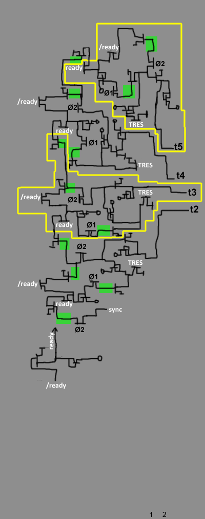
Added C simulation:
http://code.google.com/p/breaks/source/ ... TIME_REG.c
+ modified first post.

Added C simulation:
http://code.google.com/p/breaks/source/ ... TIME_REG.c
+ modified first post.
6502 addict
Re: Breaking 6502 apart
All good! Please could you link to something like
http://code.google.com/p/breaks/source/ ... 6502%2FSRC
from the first post too?
Cheers
Ed
http://code.google.com/p/breaks/source/ ... 6502%2FSRC
from the first post too?
Cheers
Ed
Re: Breaking 6502 apart
Added address bus registers simulation + modified first post with direct links.
6502 addict
Re: Breaking 6502 apart
Added missing R/W distribution tri-state, which goes from random logic to data latch.
(attached)
- More clear picture of PLA for double-checking
- Started complete 6502 schematics (WIP)
- Complete PLA simulation here:
http://code.google.com/p/breaks/source/ ... /SRC/PLA.c
(attached)
- More clear picture of PLA for double-checking
- Started complete 6502 schematics (WIP)
- Complete PLA simulation here:
http://code.google.com/p/breaks/source/ ... /SRC/PLA.c
6502 addict
Re: Breaking 6502 apart
Almost complete 6502 schematics. Only left to add missing latches and fix small errors )
I decided not to draw PLA as transistors and left it just as color diagram.
I decided not to draw PLA as transistors and left it just as color diagram.
6502 addict
Re: Breaking 6502 apart
Nice progress! I've subscribed to the RSS feed of your code project, and to the feed for your wiki.
Cheers
Ed
Cheers
Ed
Re: Breaking 6502 apart
I have a small break due to HDD failure, but thanks to Google Drive, I quickly restored all data.
Now I can present complete 6502 rev. D schematics. This part of my job is done here:
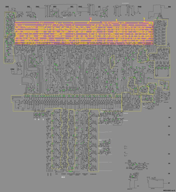
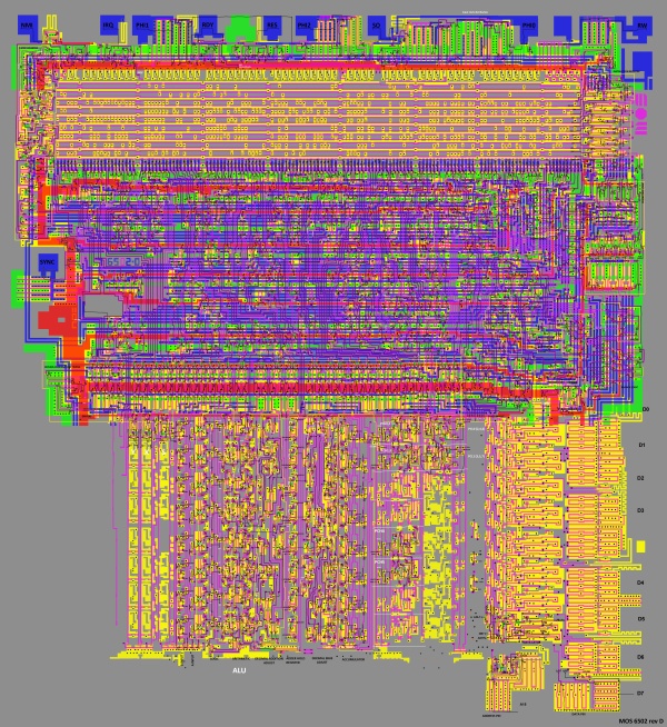
High-resoultion images can be found on google code project.
I uploaded photoshop sources here : http://ogamespec.com/6502/sources.zip (~200 MB)
And updated most interesting parts (ALU and random logic) by recent changes:
http://ogamespec.com/6502/ALU.psd
http://ogamespec.com/6502/LOGIC.psd
(remember, this is not WIP anymore)
Now I can present complete 6502 rev. D schematics. This part of my job is done here:


High-resoultion images can be found on google code project.
I uploaded photoshop sources here : http://ogamespec.com/6502/sources.zip (~200 MB)
And updated most interesting parts (ALU and random logic) by recent changes:
http://ogamespec.com/6502/ALU.psd
http://ogamespec.com/6502/LOGIC.psd
(remember, this is not WIP anymore)
6502 addict
Re: Breaking 6502 apart
Very nicely done!
Re: Breaking 6502 apart
Integrated simple assembler, to test 6502 operations in simulator.
ASM.c
ASMOPS.c
ASM.c
ASMOPS.c
6502 addict
Re: Breaking 6502 apart
I started to simulate /NMI logic and I have problems, understanding a part of circuit.
Here:
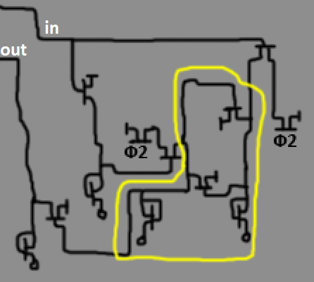
I know, this is called bistable latch, but I dont understand it at all ))
The upper MOSFET is grounded at the same time, as bottom one.. Can you explain me what happen here )
EDIT: I found solution by myself
Here:

I know, this is called bistable latch, but I dont understand it at all ))
The upper MOSFET is grounded at the same time, as bottom one.. Can you explain me what happen here )
EDIT: I found solution by myself
Code: Select all
    static nout;

    b = ~(~(in & Ф2) | nout);
    nout = (~(~in & Ф2) | b);
    out = ~nout;
6502 addict
Re: Breaking 6502 apart
I agree with the general form: it's a pair of NORs cross-coupled, with a final output inverter.
But I'm not completely sure about all the '~' operators.
I suppose you can see the result in simulation!
Cheers
Ed
But I'm not completely sure about all the '~' operators.
I suppose you can see the result in simulation!
Cheers
Ed
Re: Breaking 6502 apart
How about
Code: Select all
    static nout;

    b = ~((in & Ф2) | nout);
    nout = ~((~in & Ф2) | b);
    out = ~nout;