Bus amplifiers and terminators
-
GARTHWILSON

- Forum Moderator
- Posts: 8775
- Joined: 30 Aug 2002
- Location: Southern California
- Contact:
Re: Bus amplifiers and terminators
and that makes total sense for senarios where the total transmission-line length is very short for the rise time; but there's also distributed inductance that cannot be overcome with more mA of drive strength. That additional drive strength doesn't hurt anything as long as it is not also accompanied by edge rates that are too fast for the line length and lack of terminations (and in this case, it is apparently impossible to accomplish proper terminations).
http://WilsonMinesCo.com/ lots of 6502 resources
The "second front page" is http://wilsonminesco.com/links.html .
What's an additional VIA among friends, anyhow?
The "second front page" is http://wilsonminesco.com/links.html .
What's an additional VIA among friends, anyhow?

Re: Bus amplifiers and terminators
The problem with the stripboard is that it doesn't have so many strips to fit all of the bus lines and ground strips. Actually i barely managed to fit the data bus, control lines and 4 address lines. For the rest i use ribbon cables, and since not all modules require extended address and since it goes in only one directions, that should be a smaller problem that the backplane. As for the slew rate, could i try adjusting it with small capacitors if it is too steep?

Re: Bus amplifiers and terminators
BDD,
Thanks for the details. I had no idea the specs imply a necessary minimum rate of change. (Does it seem likely that missing that spec would merely increase the momentary power consumption? At least for a plain data input - clocks and strobes are a different case but presumably those could be conditioned by a Schmitt buffer.)
Dajgoro,
I think you're very likely to get away with it: there's the hobbyist regime, there's the professional engineer's regime, and then there's life-critical equipment. My feeling is that a lot of what you hear here is very conservative, although it is based on sound principles and practice. It's quite appropriate for a self-employed engineer.
Have a read of Quinn Dunki's blog for some well-written stories of how to make progress by experiment and adjustment. If your first attempt at a backplane isn't completely reliable, it won't kill anyone and you won't lose your job. You'll doubtless learn a lot from it. On the other hand if you waited until you understood everything as well as Dr Johnson you might never build anything.
The way to experience is to make progress: if you make mistakes you can learn from them. By all means get guidance from people more experienced, but bear in mind that they already earned their experience.
Cheers
Ed
-
GARTHWILSON
- Forum Moderator
- Posts: 8775
- Joined: 30 Aug 2002
- Location: Southern California
- Contact:
Re: Bus amplifiers and terminators
Dajgoro wrote:
The problem with the stripboard is that it doesn't have so many strips to fit all of the bus lines and ground strips. Actually i barely managed to fit the data bus, control lines and 4 address lines. For the rest i use ribbon cables, and since not all modules require extended address and since it goes in only one directions, that should be a smaller problem that the backplane.
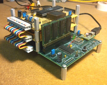
You can get ten signal conductors per inch plus grounds between them, the ribbon having 20 conductors per inch total, meaning twice what the strips on the proto board give.
Quote:
As for the slew rate, could i try adjusting it with small capacitors if it is too steep?
http://WilsonMinesCo.com/ lots of 6502 resources
The "second front page" is http://wilsonminesco.com/links.html .
What's an additional VIA among friends, anyhow?
The "second front page" is http://wilsonminesco.com/links.html .
What's an additional VIA among friends, anyhow?
Re: Bus amplifiers and terminators
For start ill try to use just BDD-s ABT ic, that i already ordered, and if i spot any issues, ill try to implement terminators or something to try make it more stable.
-
GARTHWILSON
- Forum Moderator
- Posts: 8775
- Joined: 30 Aug 2002
- Location: Southern California
- Contact:
Re: Bus amplifiers and terminators
You will have sockets, right? so you can try different parts and swap them out with minimal effort.
http://WilsonMinesCo.com/ lots of 6502 resources
The "second front page" is http://wilsonminesco.com/links.html .
What's an additional VIA among friends, anyhow?
The "second front page" is http://wilsonminesco.com/links.html .
What's an additional VIA among friends, anyhow?
-
BigDumbDinosaur

- Posts: 9429
- Joined: 28 May 2009
- Location: Midwestern USA (JB Pritzker’s dystopia)
- Contact:
Re: Bus amplifiers and terminators
BigEd wrote:
BDD,
Thanks for the details. I had no idea the specs imply a necessary minimum rate of change. (Does it seem likely that missing that spec would merely increase the momentary power consumption? At least for a plain data input - clocks and strobes are a different case but presumably those could be conditioned by a Schmitt buffer.)
Thanks for the details. I had no idea the specs imply a necessary minimum rate of change. (Does it seem likely that missing that spec would merely increase the momentary power consumption? At least for a plain data input - clocks and strobes are a different case but presumably those could be conditioned by a Schmitt buffer.)
In the data sheets that I've looked at, there usually isn't any statement as to what might happen if Δt/Δv is violated. A transient power consumption increase would happen, which, I suppose, could damage a device under certain circumstances. However, it may be that the internal logic will assume some undefined state that the chip designer either didn't foresee, or knows about but decided to ignore, since one is not supposed to violate Δt/Δv. It would analogous to an aircraft designer knowing that exceeding a certain rate of descent will cause airframe structural failure, but deciding that a warning to the pilot about the permissible limit is sufficient.
Quote:
Dajgoro,
I think you're very likely to get away with it: there's the hobbyist regime, there's the professional engineer's regime, and then there's life-critical equipment. My feeling is that a lot of what you hear here is very conservative, although it is based on sound principles and practice. It's quite appropriate for a self-employed engineer.
I think you're very likely to get away with it: there's the hobbyist regime, there's the professional engineer's regime, and then there's life-critical equipment. My feeling is that a lot of what you hear here is very conservative, although it is based on sound principles and practice. It's quite appropriate for a self-employed engineer.
Ed's right. You're not designing a mission-critical unit that is going to be used on the next voyage to the moon, where failure is not an option. Use the best design principles that you can and then accelerate the clock to see just how fast it will go. That's what I did with POC (which is stable at 12.5 MHz).
Quote:
Have a read of Quinn Dunki's blog for some well-written stories of how to make progress by experiment and adjustment.
Quinn is very good at what she does. A big plus for her is her methodical approach. It enabled her to get working VGA going with basic parts and on a patch-board, no less.
Quote:
If your first attempt at a backplane isn't completely reliable, it won't kill anyone and you won't lose your job. You'll doubtless learn a lot from it. On the other hand if you waited until you understood everything as well as Dr Johnson you might never build anything.
On the other hand, having a reasonably good grasp of the theory can make troubleshooting a lot easier, especially in cases where it just flat doesn't work, as opposed to where it sorta-works.
Quote:
The way to experience is to make progress: if you make mistakes you can learn from them. By all means get guidance from people more experienced, but bear in mind that they already earned their experience.
"Good judgment comes from experience. Experience comes from bad judgment." —anonymous
x86? We ain't got no x86. We don't NEED no stinking x86!
-
BigDumbDinosaur
- Posts: 9429
- Joined: 28 May 2009
- Location: Midwestern USA (JB Pritzker’s dystopia)
- Contact:
Re: Bus amplifiers and terminators
GARTHWILSON wrote:
and that makes total sense for senarios where the total transmission-line length is very short for the rise time; but there's also distributed inductance that cannot be overcome with more mA of drive strength.
In an ideal medium, propagation is at the approximate rate of 30 centimeters (11.81 inches) per nanosecond. That number, of course, neglects reactive effects. Seen from the far end of a bus, inductance is the limiting factor in how quickly a state change propagates. So it would behoove the designer to use a bus topology that minimizes mutual inductance. In this regard, there are plenty of models to consider. I keep turning to the parallel LVD SCSI bus as an example, on which signaling rates of 80 MHz are achieved over cables that can be as long as 12 meters with proper termination. Even the single-ended SCSI bus is able to achieve 40 MHz on a 6 meter cable.
Quote:
That additional drive strength doesn't hurt anything as long as it is not also accompanied by edge rates that are too fast for the line length and lack of terminations (and in this case, it is apparently impossible to accomplish proper terminations).
I completely agree, and ultimately, a really fast bus has to be properly terminated at both ends to avoid reflections.
x86? We ain't got no x86. We don't NEED no stinking x86!

Re: Bus amplifiers and terminators
BigEd wrote:
I had no idea the specs imply a necessary minimum rate of change. (Does it seem likely that missing that spec would merely increase the momentary power consumption?
BigDumbDinosaur wrote:
In the data sheets that I've looked at, there usually isn't any statement as to what might happen if Δt/Δv is violated. A transient power consumption increase would happen, which, I suppose, could damage a device under certain circumstances.
But the TI doc also explains how instantaneously increased dissipation during a slow transition can result in ground bounce that produces feedback opposing the input signal -- which, depending on other circumstances, might add up to a recipe for an oscillator. This is a separate issue from the thermal problem.
cheers
Jeff
In 1988 my 65C02 got six new registers and 44 new full-speed instructions!
https://laughtonelectronics.com/Arcana/ ... mmary.html
https://laughtonelectronics.com/Arcana/ ... mmary.html
-
BigDumbDinosaur
- Posts: 9429
- Joined: 28 May 2009
- Location: Midwestern USA (JB Pritzker’s dystopia)
- Contact:
Re: Bus amplifiers and terminators
Dr Jefyll wrote:
BigEd wrote:
I had no idea the specs imply a necessary minimum rate of change. (Does it seem likely that missing that spec would merely increase the momentary power consumption?
BigDumbDinosaur wrote:
In the data sheets that I've looked at, there usually isn't any statement as to what might happen if Δt/Δv is violated. A transient power consumption increase would happen, which, I suppose, could damage a device under certain circumstances.
But the TI doc also explains how instantaneously increased dissipation during a slow transition can result in ground bounce that produces feedback opposing the input signal -- which, depending on other circumstances, might add up to a recipe for an oscillator. Temperature isn't the issue.
cheers
Jeff
Oh, I had forgotten about that doc and its mention of the effects of a slow input transition on ground bounce. While ground bounce external to a device can be minimized with a careful board layout, nothing can be done about the internal die connections. So it behooves the designer (as I earlier opined) to be aware of a device's Δt/Δv and what violations might do.
x86? We ain't got no x86. We don't NEED no stinking x86!
Re: Bus amplifiers and terminators
BigDumbDinosaur wrote:
While ground bounce external to a device can be minimized with a careful board layout, nothing can be done about the internal die connections.
This idea gives me the chills, but I guess the only potential problem is if the output you've grounded fails to behave gracefully during powerup.
-- Jeff
Last edited by Dr Jefyll on Sun Sep 02, 2012 5:13 am, edited 1 time in total.
In 1988 my 65C02 got six new registers and 44 new full-speed instructions!
https://laughtonelectronics.com/Arcana/ ... mmary.html
https://laughtonelectronics.com/Arcana/ ... mmary.html
-
BigDumbDinosaur
- Posts: 9429
- Joined: 28 May 2009
- Location: Midwestern USA (JB Pritzker’s dystopia)
- Contact:
Re: Bus amplifiers and terminators
Dr Jefyll wrote:
This idea gives me the chills, but I guess it'd be OK as long as the output you've grounded behaves gracefully during powerup.
-- Jeff
-- Jeff
Sounds like a recipe for possible device failure. Simple gates like inverters probably are predictable at power-up. No telling, however, what a more complex device, say a '138 decoder, might do.
x86? We ain't got no x86. We don't NEED no stinking x86!
-
GARTHWILSON
- Forum Moderator
- Posts: 8775
- Joined: 30 Aug 2002
- Location: Southern California
- Contact:
Re: Bus amplifiers and terminators
I did that for a variable-frequency oscillator that goes to 75MHz on a 74AC-logic DIP. (I'm sure it would go higher with some changes.) I had one input and two outputs connected to ground, and two inputs and one output connected to Vcc. But yes, it was a simple inverter, not registered logic.
And speaking of oscillators, Fairchild's ap. note AN-340 tells of using non-Schmitt-trigger CMOS logic as an analog amplifier for crystal oscillators. I have not experimented, but I suspect that unlike the current spike shown in the TI document (which I only took a short look at), many CMOS logic families have both the transistors in the output totem pole semi turned off when the input is between valid logic levels, such that neither transistor is conducting very much. In the case of what the TI ap. note is showing, the extra power wasted would be approximately proportional to the percentage of the period that the waveform spends in the transition; IOW, if it's a problem, then the higher the frequency, the faster the input slew rate would need to be to keep the power dissipation down to a safe level.
However, I have seen problems when signals with noise on them take their sweet time to cross the no-man's land. Usually the solution is to use a Schmitt-trigger input, but one time I cured it by putting a capacitor at the input which actually slowed it down further but swamped out the noise. This was on a reset which did not need deep-sub-microsecond response.
http://WilsonMinesCo.com/ lots of 6502 resources
The "second front page" is http://wilsonminesco.com/links.html .
What's an additional VIA among friends, anyhow?
The "second front page" is http://wilsonminesco.com/links.html .
What's an additional VIA among friends, anyhow?
-
BigDumbDinosaur
- Posts: 9429
- Joined: 28 May 2009
- Location: Midwestern USA (JB Pritzker’s dystopia)
- Contact:
Re: Bus amplifiers and terminators
GARTHWILSON wrote:
I did that for a variable-frequency oscillator that goes to 75MHz on a 74AC-logic DIP. (I'm sure it would go higher with some changes.) I had one input and two outputs connected to ground, and two inputs and one output connected to Vcc. But yes, it was a simple inverter, not registered logic.
But Garth, don't you think all of this is a sort of band-aid approach to solving a deeper problem? If, as described in the TI publication (page 3), Δt/Δv violations are a precursor to inadvertent oscillation (which TI says can result in device fatality), it seems to this big, dumb dinosaur that every effort should be made to straighten out the problem, not mask it. At the risk of mixing metaphors, it seems to me an approach that attempts to negate the side-effects of Δt/Δv violations instead of eliminating the cause of the violations is too much like offering Tylenol to someone who is suffering from intra-cerebral hemorrhaging.
x86? We ain't got no x86. We don't NEED no stinking x86!
-
GARTHWILSON
- Forum Moderator
- Posts: 8775
- Joined: 30 Aug 2002
- Location: Southern California
- Contact:
Re: Bus amplifiers and terminators
For the VFO, the purpose was to minimize inductance to ground and Vcc in a situation where there were no problems but I wanted to maximize performance. In the case of the mechanism that can cause oscillation, it will actually improve things there, and minimize groundbounce. (Oh how I wish the original 74 logic families had started out with ground and Vcc in the middle instead of in the corners, so we wouldn't be stuck with a problem that results at speeds they did not anticipate ever reaching!) The VFO IC gets warm at the top end of its frequency range, but not at all at something like 10MHz.
The Fairchild 74AC book (printed long before TI bought them out) covers what can cause the unwanted oscillation when the input transition rate is too slow, but did not even imply that it could damage the device. To damage it, the load would have to look like a short at the oscillation frequency, and you would have to keep the input in the questionable range long enough to heat up the die enough for it to experience damage. Comparing the two companies' literature though, TI logic appears to have a problem Fairchild logic does not, which is that TI apparently can have both transistors in a totem pole saturated at the same time when the input voltage is in the middle of no-man's land. I have avoided TI over the years however because their support has always been terrible, re-confirmed recently with two projects at work. Our other engineer now thoroughly hates them. It has been sad to see TI buying up some of my favorite companies like National and Power Trends. With other companies' logic ICs, I've never damaged any except by really dumb things like connecting the power backwards or letting a screwdriver roll under the workbench computer and short out WW pins while it was running. (Yes that actually happened, and remember there's ±12V there too, not just 5V.) [Edit, correction, years later: After Fairchild was spun back off of National Semiconductor, it was On Semi that bought Fairchild, and TI bought National.]
The Fairchild book does say that their 74AC commonly have gains of 100, so the output can suddenly change states as the input slowly reaches the threshold, and if for example you have an inverter (non-Schmitt-trigger) and the input is slowly rising, the output suddenly slams down and charges the load through its ground pin, raising the input threshold because the sudden added output current rise multiplied by the inductance of the ground pin and bond wire result in a voltage that raises the input threshold enough that the input is no longer high enough to make the output low, so it goes back up, and then back down, then back up, oscillating. With a gain of 100, even 50mV change in what it perceives to be the input voltage is enough to make the output swing the entire 5V.
That's my take on it. I'd still like to learn more about various manufacturers' and logic families' detailed differences, but for now, I'm not worried about damaging parts with the input slew rate being a few ns too slow. Nor should it cause any malfunction as long as this oscillation is not in a clock signal. Dr. Johnson had a whole article about the importance of a clean clock signal and distribution method. Other signals can do whatever they want as long as they are valid and stable from the setup time before and the hold time after the relevant clock edges.
http://WilsonMinesCo.com/ lots of 6502 resources
The "second front page" is http://wilsonminesco.com/links.html .
What's an additional VIA among friends, anyhow?
The "second front page" is http://wilsonminesco.com/links.html .
What's an additional VIA among friends, anyhow?