Future plans for Dev. Board v1.2
Re: Future plans for Dev. Board v1.2
ElEctric_EyE wrote:
The 29mmx29mm SDcard connector will not fit. However, a 21mmx23mm miniSDcard connector will fit in the current board layout. I will order this part soon.
-
ElEctric_EyE
- Posts: 3260
- Joined: 02 Mar 2009
- Location: OH, USA
Re: Future plans for Dev. Board v1.2
Arlet wrote:
...Mini SD is not very popular. If you can't fit a standard SD card, I would recommend the micro SD size. It is used a lot in smart phones and other small portable equipment, so it's cheap and widely available.
There is more I wish to say, but I must wrinkle out disparities first....
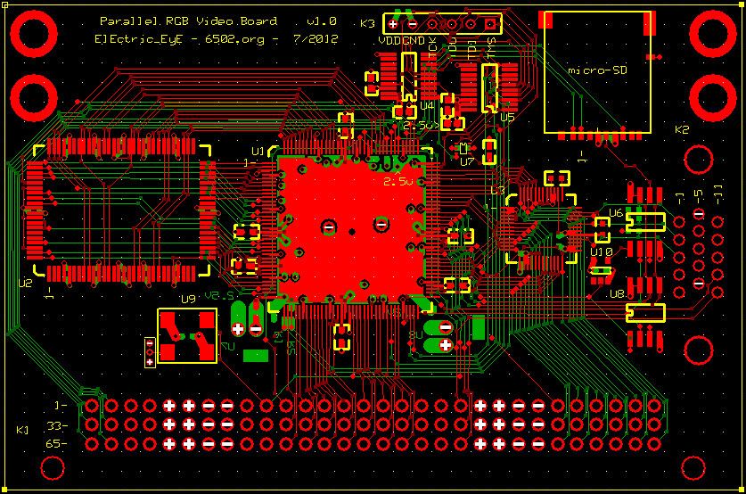
Bypass/decoupling cap's will not be labelled in this design as there is no room. Resistor's and IC's will be however.
EDIT: I will update the pic soon, due skewed VGA pin assignments. I just noticed an error there.
- GARTHWILSON
- Forum Moderator
- Posts: 8775
- Joined: 30 Aug 2002
- Location: Southern California
- Contact:
Re: Future plans for Dev. Board v1.2
EE, I wish I had paid attention to notice this sooner, but let me mention anyway that you'll get better high-speed performance if you make the power and ground pins to be evenly spaced in the 96-pin connector instead of grouping them. (I'm considering the power connections to also be virtual grounds for nanosecond rise times, since you have parallel power and ground planes and decoupling.) Ideally the return current for any given signal pin flows right next to it. If you have 24 power and ground pins evenly distributed, the return current for a particular signal pin will flow mostly through the power or ground pin closest to it, not through all 24. Space between the signal line and its nearest return makes kind of like a coil, an inductor, both radiating to, and receiving from, other lines, as well as the other effects of inductors which slow the rise times and increase groundbounce and ringing.
http://WilsonMinesCo.com/ lots of 6502 resources
The "second front page" is http://wilsonminesco.com/links.html .
What's an additional VIA among friends, anyhow?
The "second front page" is http://wilsonminesco.com/links.html .
What's an additional VIA among friends, anyhow?
-
ElEctric_EyE
- Posts: 3260
- Joined: 02 Mar 2009
- Location: OH, USA
Re: Future plans for Dev. Board v1.2
GARTHWILSON wrote:
EE, I wish I had paid attention to notice this sooner, but let me mention anyway that you'll get better high-speed performance if you make the power and ground pins to be evenly spaced in the 96-pin connector instead of grouping them...
These parallel video boards will be plugging directly into receptacles on a main board. So there will be about 1/2" space from each video board to the mainboard signal path, through the connectors.
-
ElEctric_EyE
- Posts: 3260
- Joined: 02 Mar 2009
- Location: OH, USA
Re: Future plans for Dev. Board v1.2
Doggonit, I see I've misread your post Garth!
What if I grouped all the (12) grounds together on the left side of the 96-pin connector, furthest apart from the (12) +6VDC supply pins on the right side? BTW, it's anticipated this board will use under 1000 mA at any given time, and this is distributed mostly on the 3.3V side (maybe 500mA), but some on the 1.2V FPGA core side. FPGA proms/FLASH and SDCard are negligble during normal board operation.
What if I grouped all the (12) grounds together on the left side of the 96-pin connector, furthest apart from the (12) +6VDC supply pins on the right side? BTW, it's anticipated this board will use under 1000 mA at any given time, and this is distributed mostly on the 3.3V side (maybe 500mA), but some on the 1.2V FPGA core side. FPGA proms/FLASH and SDCard are negligble during normal board operation.
- GARTHWILSON
- Forum Moderator
- Posts: 8775
- Joined: 30 Aug 2002
- Location: Southern California
- Contact:
Re: Future plans for Dev. Board v1.2
The DC current is a separate issue, and not a problem. For best AC performance, if you want 12 ground pins and 12 power pins, I would recommend something like:
so no signal pin is more than .100" from a ground or virtual ground (ie, bypassed power) pin. I strongly recommend against gouping the grounds at one end, or gouping them anywhere for that matter. Same for power, since, being bypassed, they serve as virtual grounds for the high-speed signals. Interlacing power and ground pins is best too.
Code: Select all
x x G x x x P x x x G x x x P x x x G x x x P x x x G x x x P x
P x x x G x x x P x x x G x x x P x x x G x x x P x x x G x x x
x x P x x x G x x x P x x x G x x x P x x x G x x x P x x x G x
http://WilsonMinesCo.com/ lots of 6502 resources
The "second front page" is http://wilsonminesco.com/links.html .
What's an additional VIA among friends, anyhow?
The "second front page" is http://wilsonminesco.com/links.html .
What's an additional VIA among friends, anyhow?
-
ElEctric_EyE
- Posts: 3260
- Joined: 02 Mar 2009
- Location: OH, USA
Re: Future plans for Dev. Board v1.2
Ok, I see your point. This will require the tradeoff where I will have to increase certain signal lengths in order to accomodate the pin assignments. This very small increase in inductance, due to .006" lands, should be negligible in your opinion? I always try to keeps lengths as short as possible, top priority, usually obeying the 45degree rule for high speed signals.
- GARTHWILSON
- Forum Moderator
- Posts: 8775
- Joined: 30 Aug 2002
- Location: Southern California
- Contact:
Re: Future plans for Dev. Board v1.2
Dr. Howard Johnson's article "Spread your returns" illustrates the inductance problem that results from not evenly spreading the returns among the singnal pins. His article "Who's Afraid of the Big, Bad Bend?" tells about the non-problem of 90° corners for high-speed signals in digital circuits. (I still prefer lesser angles, because of potential PCB manufacturing problems, but I don't limit myself to round numbers like 45.)
The added line length is an issue if you have to keep multiple signals arriving at their destinations simultaneously with no skew. I've seen layers added to accomplish this when the extra layers weren't needed just to get them routed. For FR-4 PCB material, figure about 136ps delay per inch, or 1.63ns per foot. I'm sure you don't have to worry about skew in this design.
The "added inductance" from a longer line is not a very accurate concept. In the transmission line, the inductance is mutual, meaning that energy taken by the signal trace's inductance is used to help the return current in the plane, meaning they cancel out. This is also why the return current does not take the shortest possible path across the ground plane, but instead takes the shape of the trace, directly under it. Traces that are against a ground plane constitute transmission lines with a characteristic impedance that can be calculated for standard FR-4 PCB material with 1-ounce copper from 16*ln(6H/(.8W + 1.4)) where H is the height of the trace above the ground plane, and W is the width of the trace, both in thousandths of an inch. If the line is terminated in its characteristic impedance, it will appear to have that impedance, purely resistive, regardless of length. Length only adds delay, and, if long enough to matter, some loss at the higher frequencies.
However, for our non-multi-GHz applications, we can usually keep the lines reasonably short and not worry about it. (The problem frequency comes way way down though with backplanes, which is why I don't recommend them.) A good rule of thumb is to terminate the transmission lines if they are longer than 2 inches per nanosecond of rise/fall time.
Ideally the ground plane would be a lot closer to any given trace than an adjacent trace would be, to keep the traces from talking to each other. There are places where there's room on your board to put more separation between the traces. Spreading the power and ground pins on the connector will probably help even more in that regard.
http://WilsonMinesCo.com/ lots of 6502 resources
The "second front page" is http://wilsonminesco.com/links.html .
What's an additional VIA among friends, anyhow?
The "second front page" is http://wilsonminesco.com/links.html .
What's an additional VIA among friends, anyhow?
- BigDumbDinosaur
- Posts: 9428
- Joined: 28 May 2009
- Location: Midwestern USA (JB Pritzker’s dystopia)
- Contact:
Re: Future plans for Dev. Board v1.2
GARTHWILSON wrote:
The DC current is a separate issue, and not a problem. For best AC performance, if you want 12 ground pins and 12 power pins, I would recommend something like:
so no signal pin is more than .100" from a ground or virtual ground (ie, bypassed power) pin. I strongly recommend against gouping the grounds at one end, or gouping them anywhere for that matter. Same for power, since, being bypassed, they serve as virtual grounds for the high-speed signals. Interlacing power and ground pins is best too.
Code: Select all
x x G x x x P x x x G x x x P x x x G x x x P x x x G x x x P x
P x x x G x x x P x x x G x x x P x x x G x x x P x x x G x x x
x x P x x x G x x x P x x x G x x x P x x x G x x x P x x x G x
x86? We ain't got no x86. We don't NEED no stinking x86!
- BigDumbDinosaur
- Posts: 9428
- Joined: 28 May 2009
- Location: Midwestern USA (JB Pritzker’s dystopia)
- Contact:
Re: Future plans for Dev. Board v1.2
ElEctric_EyE wrote:
Ok, I see your point. This will require the tradeoff where I will have to increase certain signal lengths in order to accomodate the pin assignments. This very small increase in inductance, due to .006" lands, should be negligible in your opinion? I always try to keeps lengths as short as possible, top priority, usually obeying the 45degree rule for high speed signals.
x86? We ain't got no x86. We don't NEED no stinking x86!
-
ElEctric_EyE
- Posts: 3260
- Joined: 02 Mar 2009
- Location: OH, USA
Re: Future plans for Dev. Board v1.2
Ok, I've corrected the power layout according to Garth's excellent advice based on the links to Dr. Johnson's articles!
In this update I've corrected the VGA (K2) pinout on the right and added the vertical mount FPGA Program button (S1) I'd forgotten. Also, I've included the built-in switch from the micro-SD card adapter, which will let the FPGA know if there's a card in there or not. When no card is present, the 4 lines can be used for communications to control the board. They'll be combined with other free/multi-purpose FPGA lines. Also, if no SD-Card is present, the SPI SClk is still present for the 2 64Mbit FLASHs along with their dedicated SPI signals, so they will be fully functional during mainboard communications. The mainboard is next, but...
Still working on figuring out the exact # of pins for each parallel VGA board programming.
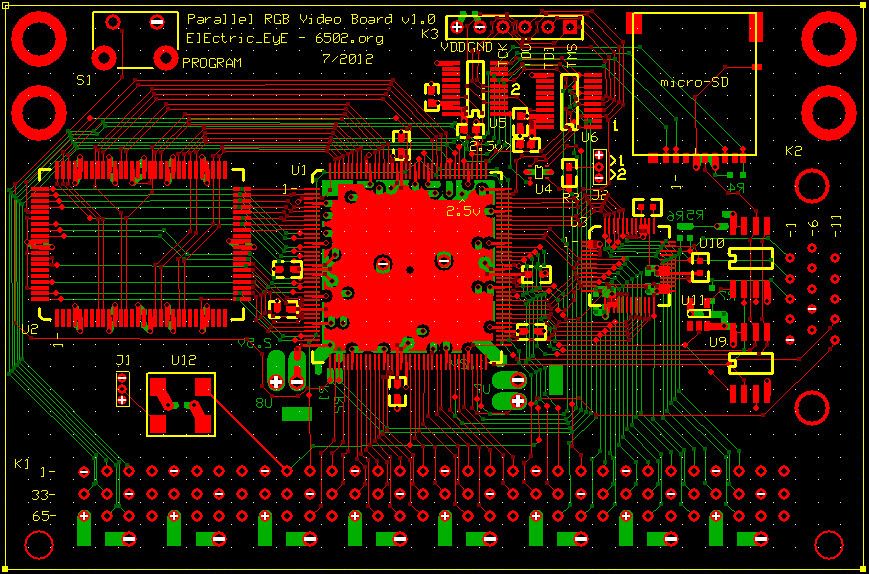
EDIT: This new updated pic has just under 350 holes. The one I had earlier was up to 358 holes due to the main connector bypass cap's, each with their own grounds. I didn't realize I was this close to the hole limit already! I don't think there's a hole counter to keep a designer on/under par. Also, I measured the pins for the main connector and VGA connector and adjusted the hole sizes accordingly. I must've misread the datasheets.
I am gaining confidence that this parallel board design will be completed by next week, and I will start a fresh thread, as promised, describing the full intent.
In this update I've corrected the VGA (K2) pinout on the right and added the vertical mount FPGA Program button (S1) I'd forgotten. Also, I've included the built-in switch from the micro-SD card adapter, which will let the FPGA know if there's a card in there or not. When no card is present, the 4 lines can be used for communications to control the board. They'll be combined with other free/multi-purpose FPGA lines. Also, if no SD-Card is present, the SPI SClk is still present for the 2 64Mbit FLASHs along with their dedicated SPI signals, so they will be fully functional during mainboard communications. The mainboard is next, but...
Still working on figuring out the exact # of pins for each parallel VGA board programming.

EDIT: This new updated pic has just under 350 holes. The one I had earlier was up to 358 holes due to the main connector bypass cap's, each with their own grounds. I didn't realize I was this close to the hole limit already! I don't think there's a hole counter to keep a designer on/under par. Also, I measured the pins for the main connector and VGA connector and adjusted the hole sizes accordingly. I must've misread the datasheets.
I am gaining confidence that this parallel board design will be completed by next week, and I will start a fresh thread, as promised, describing the full intent.
-
ElEctric_EyE
- Posts: 3260
- Joined: 02 Mar 2009
- Location: OH, USA
Re: Future plans for Dev. Board v1.2
Rechecked the design today for any lands or via's that were too close for comfort as in my one mistake in v1.1 of the devboard that affected I2C. Didn't find any. I spaced certain things even further apart actually.
Added 2 more voltage regulators. 1 for the main 3.3V, and another separate 3.3V for the videoDAC. After reading an app. note for PCB layout for Analog Devices videoDACs, I thought it would be best to have a separate supply for video. There are now 4 separate power planes within the board.
These MCP1826's have a max voltage dropout of 400mA (250mA typical), and a maximum input voltage of 6V and output current of 1A. So 5Vin through the 8 (.025" holes) pins on the main connector should provide for a reasonably good supply with plenty of current (figure extreme overkill @~7amps max!). The SRAM is the current hog of the board, potentially using up to 310mA, so main 3.3VREG placement is good.
I would like to put 6V into one of the pins of the VGA connector for the future HDMI plug-in module, so external power is not needed. It will need 5V for the hot-plug protection IC. I'm unsure which pin I could use for this purpose.
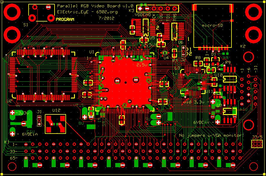
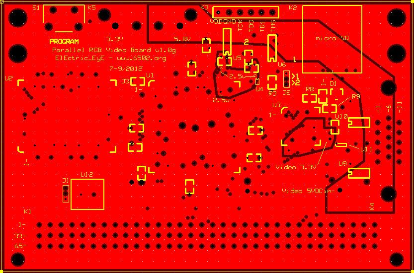
EDIT: I corrected an error where pin 9 was GND on the VGA connector. Pin 9 is now 6V and pin 10 is GND as well as VSYNC & HSYNV pin errors. Also I separated the 6Vin power planes for the option to further isolate noise. Added jumpers for connection via the main connector for other HDMI audio signals when the future HDMI module is plugged into the last VGA connector in the chain.
I am recovering holes by merging 2 FPGA bypass cap grounds that are located close to each other. This method is done now though, nothing left.
Added 2 more voltage regulators. 1 for the main 3.3V, and another separate 3.3V for the videoDAC. After reading an app. note for PCB layout for Analog Devices videoDACs, I thought it would be best to have a separate supply for video. There are now 4 separate power planes within the board.
These MCP1826's have a max voltage dropout of 400mA (250mA typical), and a maximum input voltage of 6V and output current of 1A. So 5Vin through the 8 (.025" holes) pins on the main connector should provide for a reasonably good supply with plenty of current (figure extreme overkill @~7amps max!). The SRAM is the current hog of the board, potentially using up to 310mA, so main 3.3VREG placement is good.
I would like to put 6V into one of the pins of the VGA connector for the future HDMI plug-in module, so external power is not needed. It will need 5V for the hot-plug protection IC. I'm unsure which pin I could use for this purpose.


EDIT: I corrected an error where pin 9 was GND on the VGA connector. Pin 9 is now 6V and pin 10 is GND as well as VSYNC & HSYNV pin errors. Also I separated the 6Vin power planes for the option to further isolate noise. Added jumpers for connection via the main connector for other HDMI audio signals when the future HDMI module is plugged into the last VGA connector in the chain.
I am recovering holes by merging 2 FPGA bypass cap grounds that are located close to each other. This method is done now though, nothing left.
- BigDumbDinosaur
- Posts: 9428
- Joined: 28 May 2009
- Location: Midwestern USA (JB Pritzker’s dystopia)
- Contact:
Re: Future plans for Dev. Board v1.2
ElEctric_EyE wrote:
EDIT: This new updated pic has just under 350 holes.
Don't forget that via count as holes. My POC V2 board exceeded the 650 hole limit for the Proto-Pro service, so I went on an Easter Egg hunt looking for instances where same-side traces would work. I eliminated about 20 via and got below the limit.
It would be nice if EPCB had a board statistics feature that could tell you how many holes are in the layout.
x86? We ain't got no x86. We don't NEED no stinking x86!
- GARTHWILSON
- Forum Moderator
- Posts: 8775
- Joined: 30 Aug 2002
- Location: Southern California
- Contact:
Re: Future plans for Dev. Board v1.2
EE, this is four layers, right? Since you have chainsaw lines all over the power plane, and lots of traces crossing those lines, I was going to say be sure to specify the order of layers as signal-ground-signal-power, rather than signal-ground-power-signal which would give you signal lines that aren't against a legitimate plane layer. Then I remembered you have parts on both sides, so you can't do that! I don't know what to suggest then, unless you want to add another pair of layers so that both signal layers can have their ground planes without a chopped-up power plane interfering. I don't remember Dr. Howard Johnson having any articles about that. I'll think about it and see if I can come up with anything better. I wouldn't rush to get boards made yet.
http://WilsonMinesCo.com/ lots of 6502 resources
The "second front page" is http://wilsonminesco.com/links.html .
What's an additional VIA among friends, anyhow?
The "second front page" is http://wilsonminesco.com/links.html .
What's an additional VIA among friends, anyhow?
-
ElEctric_EyE
- Posts: 3260
- Joined: 02 Mar 2009
- Location: OH, USA
Re: Future plans for Dev. Board v1.2
Well I am in a rush, but am tempered by the fact that every day modifications have been made, as well as errors. Modifcations and errors are nearing an end though!
I'm curious about the plane setup on EPCB as well...
EPCB website states that no via/hole should be closer than .007" to any other object... I can say after analyzing my error on v1.1 of the devboard, the clearance was close to .004". So EPCBs recommendations should be adhered to, and I can say that their spec's are respectable. They rec .010", but IMO one can most likely get away with .007" on a regular basis.