Video/sprites for the 65org16 Dev. board
Re: Video/sprites for the 65org16 Dev. board
ElEctric_EyE wrote:
EDIT: Added a larger pic just now, will take some time to update.
-
ElEctric_EyE
- Posts: 3260
- Joined: 02 Mar 2009
- Location: OH, USA
Re: Video/sprites for the 65org16 Dev. board
Ok, the size issue should be fixed now.
I see I missed those 3 signals. I have more than a few questions on how to properly hook this up, so please bear with me.
1) Is the vid_we signal from the bitmap module routed correctly?
2) The pixel clock (pclk) from the CS4954 module goes to the bitmap module. The system/cpu clock goes to the clk inputs of the CS4954, SDRAM, and SDRAMIF modules?
Re: Video/sprites for the 65org16 Dev. board
ElEctric_EyE wrote:
Ok, the size issue should be fixed now.
1) Is the vid_we signal from the bitmap module routed correctly?
2) The pixel clock (pclk) from the CS4954 module goes to the bitmap module. The system/cpu clock goes to the clk inputs of the CS4954, SDRAM, and SDRAMIF modules?
1) Is the vid_we signal from the bitmap module routed correctly?
2) The pixel clock (pclk) from the CS4954 module goes to the bitmap module. The system/cpu clock goes to the clk inputs of the CS4954, SDRAM, and SDRAMIF modules?
The bitmap module runs on the system/cpu clock. The same clock goes to the clk input of the CS4954. A 54 MHz clock goes into the clk54 input, and a 27 MHz clock comes out of the pclk signal, which needs to go to the video clock output of the FPGA to the CS4954 chip.
-
ElEctric_EyE
- Posts: 3260
- Joined: 02 Mar 2009
- Location: OH, USA
Re: Video/sprites for the 65org16 Dev. board
Excellent, thanks!
3) In the code for sdramif.v, there's a comment for the 'ctrl' input saying it's used for window control. It's related to the DI_CTRL[15:0]? How does this output work?
EDIT: N/M, I see 'ctrl' is related to the section you said to comment out for interfacing to an 16-bit cpu. So I don't need to use the DI_CTRL output? What is AB[15:0] used for?
Re: Video/sprites for the 65org16 Dev. board
ElEctric_EyE wrote:
3) In the code for sdramif.v, there's a comment for the 'ctrl' input saying it's used for window control. It's related to the DI_CTRL[15:0]? How does this output work?
EDIT: N/M, I see 'ctrl' is related to the section you said to comment out for interfacing to an 16-bit cpu. So I don't need to use the DI_CTRL output? What is AB[15:0] used for?
EDIT: N/M, I see 'ctrl' is related to the section you said to comment out for interfacing to an 16-bit cpu. So I don't need to use the DI_CTRL output? What is AB[15:0] used for?
Code: Select all
sdram_addr <= { ABH, AB[7:0] };
Code: Select all
sdram_addr <= AB[23:0] ;
-
ElEctric_EyE
- Posts: 3260
- Joined: 02 Mar 2009
- Location: OH, USA
Re: Video/sprites for the 65org16 Dev. board
I have enough information to hook it all up now, thanks again for the help.
My project is reaching proportions now, that I can see I am going to have trouble fitting this video portion into my project in schematic form. My next challenge will have to be to learn how to create a top level in Verilog, instead of schematic before I can see any graphics. I can get some clues from ISE's HDL translation of my schematic, and also your main.v file.
My project is reaching proportions now, that I can see I am going to have trouble fitting this video portion into my project in schematic form. My next challenge will have to be to learn how to create a top level in Verilog, instead of schematic before I can see any graphics. I can get some clues from ISE's HDL translation of my schematic, and also your main.v file.
-
ElEctric_EyE
- Posts: 3260
- Joined: 02 Mar 2009
- Location: OH, USA
Re: Video/sprites for the 65org16 Dev. board
Sorry, so many things going on in the summer months, with kids off from school I must keep them entertained for part of the day on my days off... Today I should be able to complete adding the 65Org16.b core, ZPRAM, STackRAM and a simple OSROM to your modules and hopefully see some video output. I've abandoned trying to merge my TFT project for now, with it's top level schematic. I think what will happen is I will slowly add parts of it in verilog to this new project...
Could you perchance post me your register settings for the CS4954 to save me some time?
Could you perchance post me your register settings for the CS4954 to save me some time?
Re: Video/sprites for the 65org16 Dev. board
Here's my NTSC init:
Code: Select all
reg $00 = $12
reg $01 = $12
reg $03 = $01
reg $04 = $07
reg $05 = $78
reg $10 = $1C
reg $11 = $3E
reg $12 = $F8
reg $13 = $E0
reg $14 = $43
-
ElEctric_EyE
- Posts: 3260
- Joined: 02 Mar 2009
- Location: OH, USA
Re: Video/sprites for the 65org16 Dev. board
Thanks for the quick response!
Just got done soldering in the SDRAM and .1uF bypass caps. Old TFT project, which was still loaded in FPGA FLASH, still boots up the TFT and color bars for S-Video meaning no power distribution/noise errors on this board. All other signals from FPGA to SDRAM are unused and therefore hi-impedance, except for the SDRAM /CS which I was forcing high. Taking baby steps here...
Just got done soldering in the SDRAM and .1uF bypass caps. Old TFT project, which was still loaded in FPGA FLASH, still boots up the TFT and color bars for S-Video meaning no power distribution/noise errors on this board. All other signals from FPGA to SDRAM are unused and therefore hi-impedance, except for the SDRAM /CS which I was forcing high. Taking baby steps here...
-
ElEctric_EyE
- Posts: 3260
- Joined: 02 Mar 2009
- Location: OH, USA
Re: Video/sprites for the 65org16 Dev. board
I see your values are identical to the ones I used for the color bar test pattern. But, I thought the resolution had to be specified in order to set the appropriate HSYNC and VSYNC frequencies?
My design has passed synthesis, except for the timing constraint for the CPU. Looks close though... Running smartXplorer made it pass the 10ns constraint!
I guess this is a good initial observation that with this new design with your modules, the CS4954 is outputting color bar test pattern. So at least I know the address decoding is good, the CPU is running fine with your I2C routine, and the StackRAM and ZeroPageRAM are functioning.
Re: Video/sprites for the 65org16 Dev. board
ElEctric_EyE wrote:
But, I thought the resolution had to be specified in order to set the appropriate HSYNC and VSYNC frequencies?
-
ElEctric_EyE
- Posts: 3260
- Joined: 02 Mar 2009
- Location: OH, USA
Re: Video/sprites for the 65org16 Dev. board
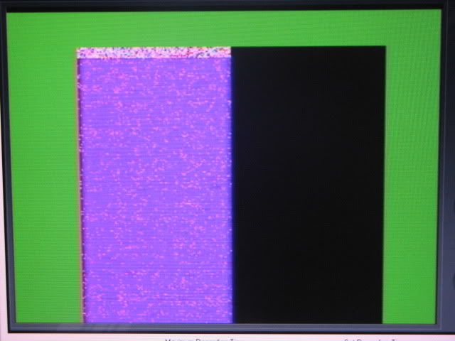
Ok, I suspected that as I didn't see any obvious registers to program. So anyway, when I disabled colorbar generation I have the beginning of graphics!!!! This is awesome when things come together so quickly. It's not perfect but most definately something to work with. I see the green border. The right half of the screen is black. Most of the left side is purple shades of pixels and on the very top, maybe 16 pixels tall, looks like regular random colored pixels one would expect. Working on getting a pic to post...
EDIT: Here it is. Bottom border is missing...

EDIT: Here it is. Bottom border is missing...

Re: Video/sprites for the 65org16 Dev. board
This is looking like something! So, is the SDRAM involved at this point?
Re: Video/sprites for the 65org16 Dev. board
I suspect the right half of the screen is black, because the bitmap is only 256 pixels wide. In your schematic you didn't hook up the 'hstretch' input to the cs4954.v module. If you tie that input to '1', the bitmap will be stretch horizontally, and it should fill the entire screen.
As far as the missing bottom, that's probably because NTSC has fewer scanlines than PAL. You should be able to fix that by adjust 'height' in the cs4954.v module. Similarly, you can adjust 'top' and 'left' to adjust the borders, so you can center the active screen on your TV/monitor.
After that, you should try to write to SDRAM from the CPU, and see if you can write on the screen.
Re: Video/sprites for the 65org16 Dev. board
BigEd wrote:
This is looking like something! So, is the SDRAM involved at this point?
6502.org wrote:
Image no longer available: http://ladybug.xs4all.nl/arlet/fpga/sdram.jpg