65Org16 CPU module / general FPGA breakout board idea

Topics relating to PALs, CPLDs, FPGAs, and other PLDs used for the support or creation of 65-family processors, both hardware and HDL.

would you buy a board with an fpga pre-programmed as a 65Org16?

Poll ended at Sat Dec 10, 2011 7:54 pm

no
4
50%
yes, if it had 40 pin DIL header and space for on board ram
2
25%
yes, if if had 80 I/Os and no space for RAM
0
No votes
yes, if it had 80 I/Os and space for RAM
1
13%
any kind at all
0
No votes
I'd buy more than one 40 pin board
0
No votes
more than one 80 pin with no RAM
0
No votes
more than one 80 pin but it must have space for RAM
0
No votes
more than one of any kind available
0
No votes
I'd buy something for sure but it's not on this list of options
1
13%
 
Total votes: 8

User avatar
BigEd
Posts: 11463
Joined: 11 Dec 2008
Location: England
Contact:

Post by BigEd »

Unfortunately, the spacing of the rows in a 64pin DIL is too tight to fit a 144 TQFP between them. Unless you decapitate a few pins as John Kortink did in his ReTuLa product.

Here's a sketch:
6502.org wrote:
Image no longer available: http://img40.imageshack.us/img40/9274/fpgatq14464dilram.png
As you see, this offers a 64 pin DIL, a 128-pin shielded option with 64 I/Os, and a 40-pin DIL option(*). I don't know if it's routable. (It's a pity the RAM pins are too tight to allow routing between them.)

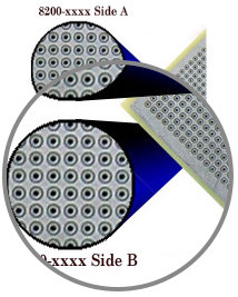
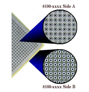
I wonder if this 64/128 pin approach will be better mechanically than the 120-pin square approach, which might be nearly impossible to unplug?

I have to say, I don't believe in the absolute need for these super-short RAM busses. Example: XO-1 runs a 4-chip SDRAM bus at 166MHz. An inch or two shouldn't be an issue. Maybe EEye's experience will tell us something, when he gets to that stage.

Cheers
Ed

(*) For the 40-pin DIL I'd ideally like to add level converters... they come in 6.2mm or 4.4mm width packages. Placeable, but I'm not sure about routeable. See page 16 of the GODIL user guide for some usage details.
User avatar
Dajgoro
Posts: 808
Joined: 08 Aug 2011
Location: Croatia
Contact:

Post by Dajgoro »

You mean something like this?

Code: Select all

 SSSSSSSSSSSSSSSSSSSSSSSSSSSSSSSS - Additional shield pins
|IOIOIOIOIOIOIOIOIOIOIOIOIOIOIOIO|
|                                |
|        64 PIN DIP SOCKET       |
|                                |
|IOIOIOIOIOIOIOIOIOIOIOIOIOIOIOIO|
 SSSSSSSSSSSSSSSSSSSSSSSSSSSSSSSS - Additional shield pins
User avatar
BigEd
Posts: 11463
Joined: 11 Dec 2008
Location: England
Contact:

Post by BigEd »

yes! That should be about the same as my sketch in the previous post.

As to how we'd order the I/Os, that's up for grabs. Generally one would want to make it easy to interface with a memory bus. As the point here is large memory, we should probably look to the signal order on DIMM or SODIMM, as well as the order on SDRAM components.

Fortunately re-ordering signals is very easy on FPGA.

Cheers
Ed
Nightmaretony
In Memoriam
Posts: 618
Joined: 27 Jun 2003
Location: Meadowbrook
Contact:

Post by Nightmaretony »

Would it be ok for a side hanging of the sub board off the 40 pin socket?

http://www.system16.com/hardware.php?id=773

bottom right on this sub-board, note the daughterboard with the overhang...
"My biggest dream in life? Building black plywood Habitrails"
User avatar
BigEd
Posts: 11463
Joined: 11 Dec 2008
Location: England
Contact:

Post by BigEd »

I expect we will do that, because the decapitation approach isn't likely to appeal.

So we end up with something like my earlier 40-pin sketch, but scaled up to 64-pin (plus optional shields, plus an embedded 40-pin.)
User avatar
Arlet
Posts: 2353
Joined: 16 Nov 2010
Location: Gouda, The Netherlands
Contact:

Post by Arlet »

Instead of a standard DIL-64, why not increase the spacing a little bit, so the FPGA fits inbetween ? It won't fit a standard IC socket, but you can use some header strips instead.

It won't be a drop-in replacement for a 64 pin IC anyway, so there's not much advantage to using a standard socket.
User avatar
Dr Jefyll
Posts: 3525
Joined: 11 Dec 2009
Location: Ontario, Canada
Contact:

Re: 65Org16 CPU module / general FPGA breakout board idea

Post by Dr Jefyll »

Code: Select all

        x x x x x x x x x x x x x x x
        x x x x x x x x x x x x x x x
        x x                       x x
        x x                       x x
        x x                       x x
        x x                       x x
        x x                       x x
        x x                       x x
        x x                       x x
        x x                       x x
        x x                       x x
        x x                       x x
        x x                       x x
        x x x x x x x x x x x x x x x
        x x x x x x x x x x x x x x x
As already noted I think, the square (rather than DIL) layout keeps traces short and consumes less board real estate. Here's a 104-pin layout. Compared to a 64-pin DIL there may be a slight mechanical issue -- it may be harder to unplug -- but that's manageable in various ways.

Re the provision of extra pins for ground plane: Rather than allowing 100% extra -- ie, one ground pin per signal pin -- I propose a smaller (but still generous) proportion. For example, 50% extra would allow two-thirds of the pins to be signal pins -- and yet every signal pin would still be adjacent to a ground pin.

BTW it seems to me that, to further reduce pin count, some of the "ground" pins could actually be the pins that carry supply voltages between the motherboard and daughterboard. Is this reasonable? In terms of reflections and other AC effects, the supply pins are ground (presuming they connect to nearby bypass cap's both on the motherboard and daughterboard).

-- Jeff
User avatar
GARTHWILSON
Forum Moderator
Posts: 8773
Joined: 30 Aug 2002
Location: Southern California
Contact:

Post by GARTHWILSON »

That's what I did on my 4Mx8 5V 10ns SRAM module which is available now. (Data sheet here.) The pinout has:

Code: Select all

   s s s s s X s s s s s s s X s s s s s s X s s
   s s X s s s s s s X s s s s s s s X s s s s s

where each "s" is a signal line and each "X" is a ground or bypassed power which for AC purposes is virtual ground; so no signal pin is more than .2" away from a ground or virtual ground.

http://WilsonMinesCo.com/
Last edited by GARTHWILSON on Fri Mar 02, 2012 5:39 am, edited 2 times in total.
User avatar
Dr Jefyll
Posts: 3525
Joined: 11 Dec 2009
Location: Ontario, Canada
Contact:

Post by Dr Jefyll »

GARTHWILSON wrote:
That's what I did on my 4Mx8 5V 10ns SRAM module
Yes, exactly. Sorry for presenting redundant material.

Code: Select all

   s s s s + - s s s s s s + - s s s s s s + - s s
   + - s s s s s s + - s s s s s s + - s s s s s s

Code: Select all

   s s s s s + - s s s s s s s + - s s s s s s s + - s s
   + - s s s s s s s + - s s s s s s s + - s s s s s s s
Here are a couple of alternative layouts, using a ratio of 3:1 and 3.5:1 signal pins per ground/power pin. (Of course even larger ratios would work.) Since the power and ground pins ( + and - ) are always adjacent, surface-mount bypass caps could be located within the header footprint (ie, between the pins).

-- Jeff
User avatar
GARTHWILSON
Forum Moderator
Posts: 8773
Joined: 30 Aug 2002
Location: Southern California
Contact:

Post by GARTHWILSON »

The ground plane will go around all the pins anyway, so if the Vcc pins are bypassed to the ground plane around them, there's no need to have them adjacent to, and paired with, the ground pins. This reduces the requirement for so many pins just to get all the signal pins suitably close to ground or virtual-ground pins.

Having chip capacitors between pins on a header would be nice, but with .040" holes (to accommodate .025" square pins), an 0603 capacitor is probably too big. 0402 is getting awfully hard to install by hand; and then you have to consider that the chip capacitors really need to be put on before the header goes on, and then getting the header on might be an extra challenge. I think I'd have to try it before I could say it was do-able. The chip capacitors might have to go outside the two rows of pins.
http://WilsonMinesCo.com/ lots of 6502 resources
The "second front page" is http://wilsonminesco.com/links.html .
What's an additional VIA among friends, anyhow?
User avatar
Dr Jefyll
Posts: 3525
Joined: 11 Dec 2009
Location: Ontario, Canada
Contact:

Post by Dr Jefyll »

GARTHWILSON wrote:
The ground plane will go around all the pins anyway, so if the Vcc pins are bypassed to the ground plane around them
On the daughterboard, yes. But it would be nice to have caps on both ends of the mating headers (male & female). The motherboard might not have a ground plane, so the option of caps between the pins may yet prove modestly helpful.

Darn dicey soldering, though, as you say. :?
User avatar
GARTHWILSON
Forum Moderator
Posts: 8773
Joined: 30 Aug 2002
Location: Southern California
Contact:

Post by GARTHWILSON »

Even if the motherboard is wire-wrapped (if WW will work at all at these speeds), it should be done on perfboard with plated-thru holes and a plane on at least one side, like this one from Twin Industries:
Image Edit, leaving the old URL to rattle their cage:
Image
This lets you solder a chip capacitor from a pin to the surrounding ground plane. This board is less than $20US for 4.5"x6.5", and less than $12US for 4"x6". 4"x10" is priced at $23.60. They also have ones with planes on both sides for the same prices, which is way cheaper than Vector used to have them.

If the mother board doesn't have a ground plane, I don't think cap.s between the pins will do much good.
http://WilsonMinesCo.com/ lots of 6502 resources
The "second front page" is http://wilsonminesco.com/links.html .
What's an additional VIA among friends, anyhow?
User avatar
GARTHWILSON
Forum Moderator
Posts: 8773
Joined: 30 Aug 2002
Location: Southern California
Contact:

Post by GARTHWILSON »

Quote:
I have to say, I don't believe in the absolute need for these super-short RAM busses. Example: XO-1 runs a 4-chip SDRAM bus at 166MHz. An inch or two shouldn't be an issue. Maybe EEye's experience will tell us something, when he gets to that stage.
Super-short is not absolutely necessary, but if they're not so short, you have to closely control the characteristic impedance of the transmission lines, terminate them properly, etc.. It's done all the time in commercial designs by engineers who are very familiar with this stuff and have an inventory of test equipment available to them that's worth more than my house; but for us hobbyists and midnight engineers, it's better to stay out of that territory by keeping connections really short and observing "good engineering practice." (Don't you just love that nebulous engineering term we use when we don't have what it takes to accurately model a circuit.)
http://WilsonMinesCo.com/ lots of 6502 resources
The "second front page" is http://wilsonminesco.com/links.html .
What's an additional VIA among friends, anyhow?
User avatar
BigEd
Posts: 11463
Joined: 11 Dec 2008
Location: England
Contact:

Post by BigEd »

To summarise where we are with this:
- not a lot of expressed interest, so even a run of 6 boards is a bit of a risk
- which makes in tempting to include everyone's wishlist

So perhaps just the preprogrammed non-volatile FPGA for a few dollars makes more sense, and let people get on with their own board design.

That is, presume that it's the FPGA/verilog which is the stumbling block, not the surface mount (or the 3V interface).

I'd be interested to hear more details from the voter who wanted 'something else'.

Cheers
Ed
Post Reply