65Org16.x Dev. Board V1.0 using a Spartan 6 XC6LX9-3TQG144
-
GARTHWILSON

- Forum Moderator
- Posts: 8775
- Joined: 30 Aug 2002
- Location: Southern California
- Contact:
At these high frequencies and fast rise times however, the main purpose of a plane is that as it runs under a trace, with no interruption, a current equal to that in the trace runs in the oposite direction in the plane, directly under the trace, eliminating common-mode signals. The return current does not take the shortest available path, but rather takes the shape of the trace. The elimination of the common-mode current cuts the radiation as well as the sensitivity to radiated signals way down, and makes a low-loss transmission line instead of an inductor and antenna. You don't have a real ground plane on this board, but hopefully it will work fine since it is so small and the traces are so short.
-
ElEctric_EyE
- Posts: 3260
- Joined: 02 Mar 2009
- Location: OH, USA
Ah, this is some great information!
But just to clarify. I have stated that this is a 4-layer miniboard pro. So with this in mind, do you guys see any problems?
The plane you see on the right is an attempt for a separate analog ground connected at one point to the digital ground plane. The plane on the left is an attempt to "shield" the USB data- and data+ signals. I just sorta threw that in at the last moment.
Last edited by ElEctric_EyE on Tue Nov 22, 2011 12:43 am, edited 2 times in total.
-
GARTHWILSON
- Forum Moderator
- Posts: 8775
- Joined: 30 Aug 2002
- Location: Southern California
- Contact:
Quote:
But just to clarify. I have stated that this is a 4-layer miniboard pro. So with this in mind, do you guys see any problems?
The plane you see on the right is an attempt for a separate analog ground connected at one point to the digital ground plane.
The plane you see on the right is an attempt for a separate analog ground connected at one point to the digital ground plane.
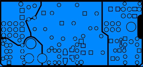
Traces should not cross the chainsaw line away from where the ground planes come together, unless you want an antenna (which is how some antennas are made on things like cell phones).
Many, many articles are available on the subject. If you want to do a search, a couple of notable authors who come to mind are Dr. Howard Johnson (guru of high-speed digital design), and Bonnie Baker who has been senior applications engineer at Texas Instruments and analog/mixed-signal applications engineering manager at Microchip, and author of "A Baker's Dozen: Real Analog Solutions for Digital Designers".
-
BigDumbDinosaur

- Posts: 9428
- Joined: 28 May 2009
- Location: Midwestern USA (JB Pritzker’s dystopia)
- Contact:
ElEctric_EyE wrote:
Ah, this is some great information!
But just to clarify. I have stated that this is a 4-layer miniboard pro. So with this in mind, do you guys see any problems?
The plane you see on the right is an attempt for a separate analog ground connected at one point to the digital ground plane. The plane on the left is an attempt to "shield" the USB data- and data+ signals. I just sorta threw that in at the last moment.
But just to clarify. I have stated that this is a 4-layer miniboard pro. So with this in mind, do you guys see any problems?
The plane you see on the right is an attempt for a separate analog ground connected at one point to the digital ground plane. The plane on the left is an attempt to "shield" the USB data- and data+ signals. I just sorta threw that in at the last moment.
With the ground and power layers covering the full board area, you have what amounts to a gigantic bypass capacitor. Also, the ground bounce effect often seen with high speed digital circuits is not an issue. I've 'scoped things on my POC unit and have noted that absolutely nothing shows up in those layers.
x86? We ain't got no x86. We don't NEED no stinking x86!
-
ElEctric_EyE
- Posts: 3260
- Joined: 02 Mar 2009
- Location: OH, USA
Ah, so I have made some bad choices in my attempt at an analog ground plane since it is overlapping either the ground plane or the power plane, not sure which?
The video using the 4954 and the audio most likely will be abit noisy. Hopefully it won't be too bad. Will have to wait and see. I think the next version I will take BDD's advice on keeping everything on the same ground plane.
Also, for the next version I would like to use a larger/or multiple Config PROMs. One that can hold 2 or 3 config's for the FPGA. Once I get an SOP for JTAG connections, I can eliminate alot of jumpers and free up some board space... The first config would write and read from certain memory locations in order to see what I/O is out there, from the attached daughterboards. Then it would write some values into the SPI Flash. Then it would go to the 2nd or 3rd config based on what is read from the SPI Flash. This will allow the design to be even more flexible. I've been reading a few datasheets, just now I can't remember where I've read about this... Will check.
Also, just got email from ExpressPCB, boards have shipped from Portland, OR.
Last edited by ElEctric_EyE on Tue Nov 22, 2011 12:43 am, edited 2 times in total.
Quote:
Also, for the next version I would like to use a larger/or multiple Config PROMs. One that can hold 2 or 3 config's for the FPGA....
Greetings
Here is some info (for spartan 2 family)
http://www.retroleum.co.uk/electronics- ... iguration/
-
ElEctric_EyE
- Posts: 3260
- Joined: 02 Mar 2009
- Location: OH, USA
Sorry, been away past 3 days, or I would've responded earlier...
bound, I've seen a Xilinx appnote where a microblaze CPU controls some of the JTAG signals, but I'm not familiar with PIC controllers or the microblaze CPUs... I'm still looking for where I originally saw that info on a multi-config setups for systems that need a self-check...
When I get hung up on one thing I pursue the project from a different angle...
I'm laying out a daughterboard(s) that will be using SRAM memory only using a Cypress 1MBx16 (16Mb). They're $40 each!...
Arlet, are you still here? How can we address maximizing memory using SDRAM. Those 16Mx16 SDRAMs are only $5 each! I could probably fit 8 of them per board...
Anyway, I'm going forward with placement for the SDRAM...
I'm not building an 8Mx16 SRAM memory board for $320.
Better to build a board fitted for 128Mx16. Pay $100 and get 3 boards, and to populate each board it only costs $40+extraneous bypass caps, headers, etc.
Last edited by ElEctric_EyE on Tue Nov 22, 2011 12:44 am, edited 2 times in total.

-
ElEctric_EyE
- Posts: 3260
- Joined: 02 Mar 2009
- Location: OH, USA
Arlet wrote:
Yes, I'm still here. Been busy with work lately. I'm not sure I understand your question. Can you elaborate ?
Great! Thought you left for good. I won't keep you long...
I know I can make 8 SRAMs work, but they're too expensive. Using SDRAMs are cheaper, but you are the only one here that seems to know what they're doing when it comes to SDRAM's.
For the memory expansion daughterboards, do you foresee a way to possibly use 8 or more SDRAM's?
Not asking for code or anything, but is this realistic?
Last edited by ElEctric_EyE on Tue Nov 22, 2011 12:44 am, edited 2 times in total.
ElEctric_EyE wrote:
Arlet wrote:
For the memory expansion daughterboards, do you foresee a way to possibly use 8 or more SDRAM's? Not asking for code or anything, but is this realistic?
-
BigDumbDinosaur
- Posts: 9428
- Joined: 28 May 2009
- Location: Midwestern USA (JB Pritzker’s dystopia)
- Contact:
Arlet wrote:
ElEctric_EyE wrote:
Arlet wrote:
For the memory expansion daughterboards, do you foresee a way to possibly use 8 or more SDRAM's? Not asking for code or anything, but is this realistic?
x86? We ain't got no x86. We don't NEED no stinking x86!
BigDumbDinosaur wrote:
What do you do about refreshing the SDRAMs?
If you use a decoder, they must be refreshed one by one, so it'll take 8 times as long.
-
ElEctric_EyE
- Posts: 3260
- Joined: 02 Mar 2009
- Location: OH, USA
Very good! I have a second board to design now. Will see how many of these memory chips I can fit on a board. Will try for 16 on 1 board. 8 on the bottom, 8 on top. Although, I can already see I would have to skimp on bypass caps if I try to fit the IC's on both sides...
That will pretty much max out the spare IO pins on the Spartan 6, with each 16Mx16 SDRAM having a separate CS, as there are 20 spare IO pins now.
This memory expansion daughterboard would be one option for a user.
I'll work on it during my spare time waiting for parts.
Boards came today and they look awesome! Still looking them over and have to test for shorts between layers and stuff like that, but man I guess they don't kid when their program measures down to the .001". It is exact. Some vias very close to each other and some close to other lines I though might be shorted, but they are clean. Whew! This ExpressPCB company is awesome! So far I fitted the Spartan 6 on the custom template I made from the datasheet measurements and it fit perfect, so hopefully all the other custom connectors, headers, and IC's will fit too. Stuff I am ordering now.
Last edited by ElEctric_EyE on Tue Nov 22, 2011 12:44 am, edited 2 times in total.

-
ElEctric_EyE
- Posts: 3260
- Joined: 02 Mar 2009
- Location: OH, USA
BigEd wrote:
...Have you figured out the loads and the effect on timing for this 16-chip bus? It wouldn't be surprising to find that a larger memory system will run slower.
Cheers
Ed
I agree, thankfully this is an optional board. Even the onboard SDRAM is optional, one just needs to tie the line high inside the FPGA....
I don't know how to figure bus loading and the effect on speeds. I'd be willing to learn... What I plan to do is make a board that can fit 16 SDRAMs, and start off with one SDRAM (actually in addition to the one on the mainboard) and do some tests, and keep adding one until failures start occurring. This is just abit in the future though.
Hopefully, this weekend I can begin soldering parts I just ordered for the mainboard. Had a little difficulty finding the 1.2V regulator in the package I needed with Digi-Key. Luckily Mouser had 35 in stock.
Last edited by ElEctric_EyE on Tue Nov 22, 2011 12:45 am, edited 2 times in total.