
In my case, I made my 6502 core in order to recreate my old 6502-based Acorn Atom computer, which was the first computer I ever had, and used to learrn 6502 assembly language. My Atom only had 12KB of memory, so to make things easy I figured I would use the built-in block RAMs instead of increasing complexity and using external SRAMs.
Now, I think it should be possible to use external SRAM/Flash, using DDR flip flops, but I've never tried it myself. I'm still interested in trying it some time, but I'm too busy right now.
Using external SRAM that can also be used as VGA frame buffer is even harder, because of the coordination of the two different accesses. I was actually considering not having direct CPU access to the VGA memory, but putting in a special 2D graphics controller which also serves as an accelerator for high bandwidth operations, like scrolling the screen. So, instead of the 6502 reading/writing all the pixels, it would just send a simple command to move a rectangle from location A to location B. Needless to say, this is quite a big project.
A 6502 SoC Project using a Spartan 3 FPGA

(This became a bit of a ramble but I hope it's still worth posting)
As I'm sure you know, the old-school method was for the video hardware to use the same RAM as the CPU, but using the unused first phase of each CPU cycle. The RAM needs to have a cycle time half that of the CPU, or in other words the CPU can only run at half the speed of the RAM. For that cost, you don't need any complex logic or clocking to share the RAM between the two subsystems. (Your comment on DDR perhaps means exactly this?)
I see there's a VHDL model or two for a 6845 CRTC, which would be a typical video controller in those days.
The Acorn Electron approach was to gate the CPU clock, stalling the CPU during pixel output in high-resolution modes, and causing high interrupt latency (pdf). (It had 4-bit wide RAM, so it also runs slow during RAM access, and at top speed only for ROM access.)
On the subject of having a smart video controller which takes higher-level commands from the CPU side, the BBC Micro architecture has a VDU command interpreter, so that control codes written to the OS output routine can cause graphics operations.
With the Tube chip and protocol, the machine with the VDU gets those output bytes through a FIFO from the main processor (which has the Tube as the only peripheral.) Now you have two CPUs and two memory systems: one is for I/O including graphics and the other is for the real work. If we suppose only a single memory interface on the FPGA than this means the I/O processor has to make do with block RAM. In which case, the 'graphics subsystem' becomes a BBC micro - which is also available in HDL.
So, yes, a smart graphics controller is a complex project, but possibly a project which already exists in some form.
Hmm, that's true.
The simplest thing to do is to run the CPU slower - other than that, it's a question of being able to stall it or gate the clock, with or without some layer of buffer or cache. (We've mentioned before ideas of using full-speed block RAM at least for page zero and one, or for a cache. And block RAM for at least some of the ROM.)
I suppose it would be much easier to make a safe clock-gating circuit than to implement RDY in your pipeline?
I'm thinking of targetting the OHO GOP module, which has an R1LV0408CSA-5SI (55ns) SRAM on board. That's 18MHz as an upper bound on cycle time and as you say possibly as little as half that in practice.
-
GARTHWILSON

- Forum Moderator
- Posts: 8773
- Joined: 30 Aug 2002
- Location: Southern California
- Contact:
Not for me, as the module has a fixed circuit. More generally, it's an option if the graphics subsystem is on a separate FPGA, or if the FPGA has enough pins to bring both ports into play. If the memory is relatively narrow that might work out.
I think the usual solution is to have a single memory interface, but for it to very wide, and to have prefetch buffers or caches inboard of the memory interface, and for memory accesses to read or write entire packets of data for each access (several words per access)
All of which adds complexity.
Probably the simplest is to have the graphics subsystem on a separate FPGA with a private memory, or to have a small enough system that it can be brought entirely onboard, or entirely outboard like an actual 6845. A character-based system would certainly fit onboard.
-
ElEctric_EyE
- Posts: 3260
- Joined: 02 Mar 2009
- Location: OH, USA
Garth, I've looked at dual-port RAMs too (external to the FPGA), and most of the larger ones like 2M have wide datapaths, like 18 or 36 bits, and come in 400+pin BGA packages... The smaller 8 bit data path devices are very limited in memory depth. I've seen 128K MAX on Digikey.com. Maybe more searching is in order...
I think we're on to something there with the dualport Rams... But I'd like to know why the big discrepancy between the depth and width of dual port RAM's, synchronous or asynchronous...
The FPGA I'm using, XC3S400, has a maximum of 32K internal RAM... It shows how limited these FPGA's are, when it comes to internal RAM... The block RAMs are probably best used for zeropage/stack/+more than a few data registers and the core's ROM.
To all: What if the VGA interface is a write to only type of interface? Why would one need to read from a display anyway? Unless it's a gaming type system where you need a sprite type collision register?...
I'm gonna check out some arcade schematics and parts for ideas...
-
ElEctric_EyE
- Posts: 3260
- Joined: 02 Mar 2009
- Location: OH, USA
I couldn't find a decent sized dual port SRAM for a video graphics application. So now I am on a different tangent of thought...
It'd be nice if Xilinx could have another FPGA family that would have a high density SRAM with some logic to control it, instead of high density logic and just a little RAM. Finally put DRAM to rest.
BigEd, thank you for your ramblings!, I think we all need to ramble more so I'm gonna, and try one of those 6845 cores, maybe search for more... But since the video RAM will not be part of the FPGA, I do need to figure out the READ timing of Arlet's 6502 Core (his core is most likely THE fastest core, if you can do everything internal), which I intend to do with the FLASH I mentioned before, hopefully in the next couple days. The WRITE timing I have already proven with the TFT display and max'd it (the TFT display) out @38MHz...
Just so I don't mislead anyone following this thread, I am developing a write only type of graphics system that will transfer information to a user at the highest speeds. The other side of the spectrum would be a gaming type system that would need to read & write to the video RAM, because their user is controlling sprites and interacting every millisecond.
In my concept, the CPU only writes to the video RAM based on input from keyboard only. Data inputted from the FLASH/SD Card is only allowed under command from the keyboard. The video controller only reads from the video RAM and constantly shifts out pixel data. The easiest type of data transfer from the CPU to video RAM would be during an inactive Display Enable. Initially, I'm sure this would work, but I would like to delve abit further after I get to this point.
Reading from display RAM is also necessary when you want to move areas around, for example when scrolling.
By the way, it's easy to make a text-only VGA generator in the FPGA itself. You can have a 80*25 screen in a single block RAM, and use another one for the character ROM (8x16 font, 128 chars). Using internal memory allows dual-port access, so it's really easy to interface with the 6502 core.
By the way, it's easy to make a text-only VGA generator in the FPGA itself. You can have a 80*25 screen in a single block RAM, and use another one for the character ROM (8x16 font, 128 chars). Using internal memory allows dual-port access, so it's really easy to interface with the 6502 core.
-
ElEctric_EyE
- Posts: 3260
- Joined: 02 Mar 2009
- Location: OH, USA
Arlet wrote:
By the way, it's easy to make a text-only VGA generator in the FPGA itself...
Here's the code from BigEd's second link to pacedev. I had to clean it up. There were just a few syntax errors ISE did not understand.
Is there a way to make a scrolling window for the code?
Code: Select all
// CRTC6845(HD46505) CORE
//
// Version : beta 4
//
// Copyright(c) 2004 Katsumi Degawa , All rights reserved.
// Copyright(c) 2004 Tatsuyuki Satoh , All rights reserved.
//
// Important !
//
// This program is freeware for non-commercial use.
// An author does no guarantee about this program.
// You can use this under your own risk.
//
// VerilogHDL model of MC6845(HD46505) compatible CRTC.
// This was made for FPGA-GAME(ROCK-OLA).
// Therefore. There is a limitation in the function.
// 1. This doesn't implement interlace mode.
// 2. This doesn't implement light pen detection founction.
// 3. This doesn't implement cursor control founction.
//
// 4. This doesn't implement display sque (HD46505SP)
// 5. This doesn't support case Nht==0
//
// File History
// 2005. 4. 5 by T.satoh
// bugfix port size mismatch
// 2005. 1.13 by T.satoh
// bugfix VSYNC pulse width (line to raster)
// bugfix NEXT_R_RA bit size mismatch.
// 2004.12. 9 by T.satoh
// rewrite source with minimize code. (178 -> 119 slice to Spartan3 with Area optimize)
// bugfix , bypass wite register 10H-1FH ( R_ADR width change 5bit from 4bit).
// fix register mismatch width W_Nr,O_Nr,Nvt,Nvd and Nvsp.
// change R_V_CNT width 9bit to 7bit.
//
// 2004.10.23 First release
//--------------------------------------------------------------------------------------
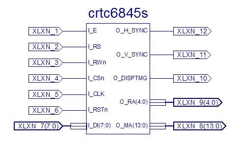
module crtc6845s(
// INPUT
I_E,
I_DI,
I_RS,
I_RWn,
I_CSn,
I_CLK,
I_RSTn,
// OUTPUT
O_RA,
O_MA,
O_H_SYNC,
O_V_SYNC,
O_DISPTMG
);
input I_E;
input [7:0]I_DI;
input I_RS;
input I_RWn;
input I_CSn;
input I_CLK;
input I_RSTn;
output [4:0]O_RA;
output [13:0]O_MA;
output O_H_SYNC;
output O_V_SYNC;
output O_DISPTMG;
wire [7:0]W_Nht;
wire [7:0]W_Nhd;
wire [7:0]W_Nhsp;
wire [3:0]W_Nhsw;
wire [6:0]W_Nvt;
wire [4:0]W_Nadj;
wire [6:0]W_Nvd;
wire [6:0]W_Nvsp;
wire [3:0]W_Nvsw;
wire [4:0]W_Nr;
wire [13:0]W_Msa;
wire W_Vmode;
wire W_IntSync;
wire [1:0] W_DScue;
wire [1:0] W_CScue;
mpu_if mpu_if(
.I_RSTn(I_RSTn),
.I_E(I_E),
.I_DI(I_DI),
.I_RS(I_RS),
.I_RWn(I_RWn),
.I_CSn(I_CSn),
.O_Nht(W_Nht),
.O_Nhd(W_Nhd),
.O_Nhsp(W_Nhsp),
.O_Nhsw(W_Nhsw),
.O_Nvt(W_Nvt),
.O_Nadj(W_Nadj),
.O_Nvd(W_Nvd),
.O_Nvsp(W_Nvsp),
.O_Nvsw(W_Nvsw),
.O_Nr(W_Nr),
.O_Msa(W_Msa),
.O_VMode(W_Vmode),
.O_IntSync(W_IntSync),
// HD46505-SP only
.O_DScue(W_DScue),
.O_CScue(W_CScue)
);
crtc_gen crtc_gen(
.I_CLK(I_CLK),
.I_RSTn(I_RSTn),
.I_Nht(W_Nht),
.I_Nhd(W_Nhd),
.I_Nhsp(W_Nhsp),
.I_Nhsw(W_Nhsw),
.I_Nvt(W_Nvt),
.I_Nadj(W_Nadj),
.I_Nvd(W_Nvd),
.I_Nvsp(W_Nvsp),
.I_Nvsw(W_Nvsw),
.I_Nr(W_Nr),
.I_Msa(W_Msa),
.O_RA(O_RA),
.O_MA(O_MA),
.O_H_SYNC(O_H_SYNC),
.O_V_SYNC(O_V_SYNC),
.O_DISPTMG(O_DISPTMG)
);
endmodule
module mpu_if(
I_RSTn,
I_E,
I_DI,
I_RS,
I_RWn,
I_CSn,
O_Nht,
O_Nhd,
O_Nhsp,
O_Nhsw,
O_Nvt,
O_Nadj,
O_Nvd,
O_Nvsp,
O_Nvsw,
O_Nr,
O_Msa,
O_DScue,
O_CScue,
O_VMode,
O_IntSync
);
input I_RSTn;
input I_E;
input [7:0]I_DI;
input I_RS;
input I_RWn;
input I_CSn;
output [7:0]O_Nht;
output [7:0]O_Nhd;
output [7:0]O_Nhsp;
output [3:0]O_Nhsw;
output [6:0]O_Nvt;
output [4:0]O_Nadj;
output [6:0]O_Nvd;
output [6:0]O_Nvsp;
output [3:0]O_Nvsw;
output [4:0]O_Nr;
output [13:0]O_Msa;
output [1:0] O_DScue;
output [1:0] O_CScue;
output O_VMode;
output O_IntSync;
reg [4:0]R_ADR;
reg [7:0]R_Nht;
reg [7:0]R_Nhd;
reg [7:0]R_Nhsp;
reg [7:0]R_Nsw;
reg [6:0]R_Nvt;
reg [4:0]R_Nadj;
reg [6:0]R_Nvd;
reg [6:0]R_Nvsp;
reg [7:0]R_Intr;
reg [4:0]R_Nr;
reg [5:0]R_Msah;
reg [7:0]R_Msal;
assign O_Nht = R_Nht;
assign O_Nhd = R_Nhd;
assign O_Nhsp = R_Nhsp;
assign O_Nhsw = R_Nsw[3:0];
assign O_Nvt = R_Nvt;
assign O_Nadj = R_Nadj;
assign O_Nvd = R_Nvd;
assign O_Nvsp = R_Nvsp;
assign O_Nvsw = R_Nsw[7:4];
assign O_Nr = R_Nr;
assign O_Msa = {R_Msah,R_Msal};
assign O_VMode = R_Intr[1];
assign O_IntSync = R_Intr[0];
// HD46505-SP only
assign O_DScue = R_Intr[5:4]; // disp scue 0,1,2 or OFF
assign O_CScue = R_Intr[7:6]; // cursor scue 0,1,2 or OFF
always@(negedge I_RSTn or negedge I_E)
begin
if(~I_RSTn) begin
// this is currently set for "non-interlace MODE 7"
// - it's a fudge because this controller doesn't support interlace
R_Nht <= 8'h3F; // 0
R_Nhd <= 8'h28; // 1
R_Nhsp <= 8'h33; // 2
R_Nsw <= 8'h24; // 3
R_Nvt <= 7'h1E; // 4
R_Nadj <= 5'h02; // 5
R_Nvd <= 7'h19; // 6
R_Nvsp <= 7'h1B; //1C; // 7
R_Intr <= 8'h91; //93; // 8
R_Nr <= 5'h09; //12; // 9
R_Msah <= 6'h28; // 12
R_Msal <= 8'h00; // 13
end else
if(~I_CSn)begin
if(~I_RWn)begin
if(~I_RS)begin
R_ADR <= I_DI[4:0];
end else begin
case(R_ADR)
5'h0 : R_Nht <= I_DI ;
5'h1 : R_Nhd <= I_DI ;
5'h2 : R_Nhsp <= I_DI ;
5'h3 : R_Nsw <= I_DI ;
5'h4 : R_Nvt <= I_DI[6:0] ;
4'h5 : R_Nadj <= I_DI[4:0] ;
5'h6 : R_Nvd <= I_DI[6:0] ;
5'h7 : R_Nvsp <= I_DI[6:0] ;
5'h8 : R_Intr <= I_DI[7:0] ;
5'h9 : R_Nr <= I_DI[4:0] ;
5'hC : R_Msah <= I_DI[5:0] ;
5'hD : R_Msal <= I_DI ;
default:;
endcase
end
end
end
end
endmodule
module crtc_gen(
I_CLK,
I_RSTn,
I_Nht,
I_Nhd,
I_Nhsp,
I_Nhsw,
I_Nvt,
I_Nadj,
I_Nvd,
I_Nvsp,
I_Nvsw,
I_Nr,
I_Msa,
O_RA,
O_MA,
O_H_SYNC,
O_V_SYNC,
O_DISPTMG
);
input I_CLK;
input I_RSTn;
input [7:0]I_Nht;
input [7:0]I_Nhd;
input [7:0]I_Nhsp;
input [3:0]I_Nhsw;
input [6:0]I_Nvt;
input [4:0]I_Nr;
input [4:0]I_Nadj; // (I_Nadj-1 <= I_Nr) is Support. (I_Nadj-1 > I_Nr) is Not Support.
input [6:0]I_Nvd;
input [6:0]I_Nvsp;
input [3:0]I_Nvsw;
input [13:0]I_Msa;
output [4:0]O_RA;
output [13:0]O_MA;
output O_H_SYNC;
output O_V_SYNC;
output O_DISPTMG;
reg [7:0]R_H_CNT;
reg [6:0]R_V_CNT;
reg [4:0]R_RA;
reg [13:0]R_MA;
reg R_H_SYNC,R_V_SYNC;
reg R_DISPTMG ,R_V_DISPTMG;
reg R_LAST_LINE;
// next count value (cnt+1)
wire [7:0] NEXT_R_H_CNT = (R_H_CNT+8'h01);
wire [6:0] NEXT_R_V_CNT = (R_V_CNT+7'h01);
wire [4:0] NEXT_R_RA = R_RA + 1;
// h return trigger
wire W_HD = (R_H_CNT==I_Nht);
// v return trigger
wire W_VD = (R_V_CNT==I_Nvt);
wire W_ADJ_C = R_LAST_LINE & (NEXT_R_RA==I_Nadj);
wire W_VCNT_RET = ((R_RA==I_Nr) & (I_Nadj==0) & W_VD) | W_ADJ_C;
// RA return trigger
wire W_RA_C = (R_RA==I_Nr) | W_ADJ_C;
// sync trigger
wire W_HSYNC_P = (NEXT_R_H_CNT == I_Nhsp);
wire W_HSYNC_W = (NEXT_R_H_CNT[3:0] == (I_Nhsp[3:0]+I_Nhsw) );
wire W_VSYNC_P = (NEXT_R_V_CNT == I_Nvsp ) & W_RA_C;
wire W_VSYNC_W = (NEXT_R_RA[3:0]==I_Nvsw);
// disp trigger
wire W_HDISP_N = (NEXT_R_H_CNT==I_Nhd);
wire W_VDISP_N = (NEXT_R_V_CNT==I_Nvd) & W_RA_C;
//output assign
assign O_H_SYNC = R_H_SYNC;
assign O_V_SYNC = R_V_SYNC;
assign O_RA = R_RA;
assign O_MA = R_MA;
assign O_DISPTMG = R_DISPTMG;
// MA MAX = 14'h3FFF ---------------------
reg [13:0] R_MA_C;
always@(negedge I_CLK or negedge I_RSTn)
begin
if(! I_RSTn)begin
R_MA <= 14'h0000;
R_MA_C <= 14'h0000;
R_H_CNT <= 8'h00;
R_H_SYNC <= 0;
R_RA <= 5'h00;
R_V_CNT <= 7'h00;
R_LAST_LINE <= 1'b0;
R_V_SYNC <= 0;
R_V_DISPTMG <= 1'b0;
R_DISPTMG <= 1'b0;
end
else begin
// H CNT
R_H_CNT <= W_HD ? 8'h00 : NEXT_R_H_CNT;
// MA
R_MA <= W_HD ? R_MA_C : R_MA + 1;
// MA return address
if(W_RA_C & (R_H_CNT==I_Nhd) )
R_MA_C <= W_VCNT_RET ? I_Msa : R_MA;
// HSYNC
if(W_HSYNC_P) R_H_SYNC <= 1'b1;
else if(W_HSYNC_W) R_H_SYNC <= 1'b0;
// H RETURN
if(W_HD)
begin
// RA
R_RA <= W_RA_C ? 5'h00 : NEXT_R_RA;
// VSYNC
if(W_VSYNC_P) R_V_SYNC <= 1'b1;
else if(W_VSYNC_W) R_V_SYNC <= 1'b0;
if(W_RA_C)
begin
// for adjust line
R_LAST_LINE <= W_VD;
// V CNT
R_V_CNT <= W_VCNT_RET ? 7'h00 : NEXT_R_V_CNT;
end
end
// V DISPTMG (next line)
if(W_VCNT_RET) R_V_DISPTMG <= 1'b1;
else if(W_VDISP_N) R_V_DISPTMG <= 1'b0;
// H & V DISPTMG
if(W_HD) R_DISPTMG <= R_V_DISPTMG;
else if(W_HDISP_N) R_DISPTMG <= 1'b0;
end
end
endmodule
Looks like DISPTMG is Display Enable? And there's no DataOut so the registers are write only.
(I don't think you can force a code display to scroll - your post is as long as you choose to make it!)
The datasheet contains a block diagram of how a 6845 might be used.
The O_DISPTMG stands for 'Display Timing' - in the datasheet it's DE, meaning 'Display Enable' and yes, it signals the active period. That allows you to output a border colour, which was useful when displaying to a TV.
The datasheet contains a block diagram of how a 6845 might be used.
The O_DISPTMG stands for 'Display Timing' - in the datasheet it's DE, meaning 'Display Enable' and yes, it signals the active period. That allows you to output a border colour, which was useful when displaying to a TV.
-
ElEctric_EyE
- Posts: 3260
- Joined: 02 Mar 2009
- Location: OH, USA
@BigEd. I could've sworn I've scrolled through some code in a window maybe in the programming section here on 6502.org...
Just to link to a relevant thread! The links are still alive. Evidently, there are still places that sell the Hitachi equivalent (HD46505) of the MC6845 silicon. I still have the ones I bought in that thread. Any buyers?
Now I'm going to put them into an FPGA. Man, this is awesome!
Also, tomorrow I wirewrap the FLASH. Then test the read patterns and write them the TFT display for observation.
-
ElEctric_EyE
- Posts: 3260
- Joined: 02 Mar 2009
- Location: OH, USA
Today, I accomplished a few things:
Soldered the Flash and wired the VCC's & GND.
Tightened up the address decoding. A0 is the only one left floating due to the TFT's need of A0.
Added the signals needed to qualify a write of the databus going to the TFT Display. Before the Flash, it was the only device on the 6502 Databus out.
Added separate Write and Read data buses for the Flash.
Got rid of the 16K internal RAM2 meant for the Flash copy window. The window is now 1K@$0400-$07FF. 4K ROM still the same @$F000-$FFFF, so is the zero-page/stack/variable register area @$0000-$03FF.
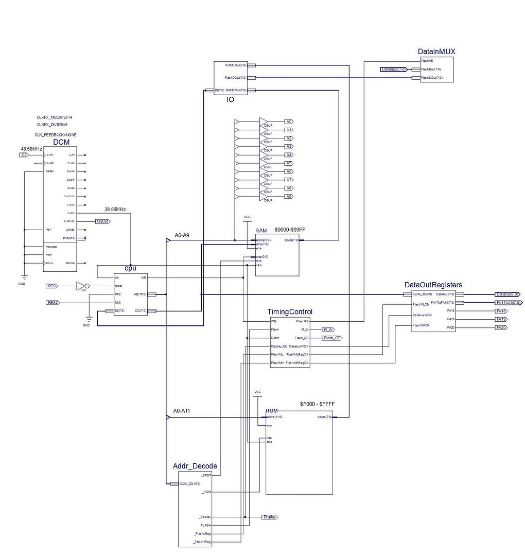
I've had to change quite abit of the schematic. There are I/O buses cropping up everywhere! 2 data buses for the flash, 1 for the TFT. I am beginning to understand why the pin count is so high on these FPGA's. I'm learning that each typical external parallel memory/peripheral needs 2 buses each. One for reading, 1 for writing.
So after adding all this one step at a time, using the same constraints, it worked almost perfect. All the additions were transparent, which is what I was hoping for. The screen does locks up randomly after more than a few screens of data have been sent, just like before I lowered the DRIVE constraint to 4 mA. And I don't feel comfortable lowering it more, so...
Now is the time for all good men to come to the aid of their country! Uh, I mean to say, now I'm gonna add some bypass cap's. Unavoidable now.
Still very short on resources being used on this XC3S400 beast! This is the top_level schematic. Will post a pic of resource usage after I have 100% success with the Flash and TFT working together... Sorry for the large pic but I think it's necessary to see the detail, plus BigEd said I could. :
:
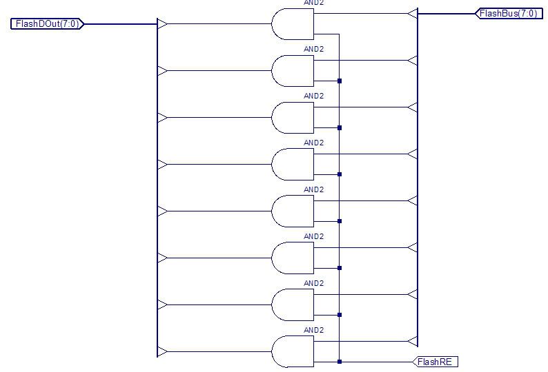
The DataInMUX symbol in the above schematic (Thanks to Tony & Garth, I had a flashback to this): I had to make the databus inputs from the external Flash be all '0' when it was inactive, in order to conform the the internal data structure. Initially, I was thinking of 8x 2to1 MUX's, but this worked very nicely.
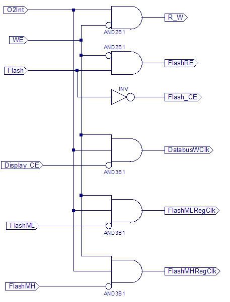
Timing control: O2Int is the 38.86MHz 02 internal from the DCM. R_W goes the the TFT. Flash, Display_CE($C000-$C001), FlashML($C002), and Flash MH($C004) are from simple addressing decoding. DatabusWClk, FlashMLRegClk, and FlashMHRegClk are clock signals going to flip flops.
Data Out Registers:
Soldered the Flash and wired the VCC's & GND.
Tightened up the address decoding. A0 is the only one left floating due to the TFT's need of A0.
Added the signals needed to qualify a write of the databus going to the TFT Display. Before the Flash, it was the only device on the 6502 Databus out.
Added separate Write and Read data buses for the Flash.
Got rid of the 16K internal RAM2 meant for the Flash copy window. The window is now 1K@$0400-$07FF. 4K ROM still the same @$F000-$FFFF, so is the zero-page/stack/variable register area @$0000-$03FF.
I've had to change quite abit of the schematic. There are I/O buses cropping up everywhere! 2 data buses for the flash, 1 for the TFT. I am beginning to understand why the pin count is so high on these FPGA's. I'm learning that each typical external parallel memory/peripheral needs 2 buses each. One for reading, 1 for writing.
So after adding all this one step at a time, using the same constraints, it worked almost perfect. All the additions were transparent, which is what I was hoping for. The screen does locks up randomly after more than a few screens of data have been sent, just like before I lowered the DRIVE constraint to 4 mA. And I don't feel comfortable lowering it more, so...
Now is the time for all good men to come to the aid of their country! Uh, I mean to say, now I'm gonna add some bypass cap's. Unavoidable now.
Still very short on resources being used on this XC3S400 beast! This is the top_level schematic. Will post a pic of resource usage after I have 100% success with the Flash and TFT working together... Sorry for the large pic but I think it's necessary to see the detail, plus BigEd said I could.
The DataInMUX symbol in the above schematic (Thanks to Tony & Garth, I had a flashback to this): I had to make the databus inputs from the external Flash be all '0' when it was inactive, in order to conform the the internal data structure. Initially, I was thinking of 8x 2to1 MUX's, but this worked very nicely.
Timing control: O2Int is the 38.86MHz 02 internal from the DCM. R_W goes the the TFT. Flash, Display_CE($C000-$C001), FlashML($C002), and Flash MH($C004) are from simple addressing decoding. DatabusWClk, FlashMLRegClk, and FlashMHRegClk are clock signals going to flip flops.
Data Out Registers:
-
ElEctric_EyE
- Posts: 3260
- Joined: 02 Mar 2009
- Location: OH, USA
I was trying to make too many changes at once..It seems I was a little too excited about posting schematics about what seemed to be working, and after further testing, repeatability was not there. Again it's something to do with ISE, only because after changing so many design details, it still was clearing the screen successfully. It is mainly my fault, because I fell back to my old ways of mixing clock signals with logic level signals. Ah, but this is "synthesis" versus real world TTL/CMOS logic. This old school type of thinking is not acceptable. The poster is not me, but someone like me...
Parts of the schematic have changed but from now on I plan to post schematics only at the end of a "chapter". This chapter being reading and writing and erasing the Flash.
Enough of the explanations, now on to the progress!
I got back to the point of clearing the screen @38MHz with the Flash fully wired to the FPGA and pin assignments locked, though no interaction with the Flash yet. O2 clock has been removed from Timing control. DataInMUX AND gates were replaced with 2to1MUX's. Most importantly the internal data bus goes straight out of the FPGA through OBUF's, not through a FF.
In preparation for reading from the Flash, I lowered the O2internal speed to 12MHz while using the same screen color changing software, and am seeing correct data being displayed. Now I am working on the FA10-FA20 Flash address ports and Flash_CE signals.
P.S. I really want to start the video portion next. I've got some neat ideas I would like to share, albeit very general ideas, but I can tell you for sure that it will have it's own dedicated FPGA to keep the 6502's as fast as possible...
-
ElEctric_EyE
- Posts: 3260
- Joined: 02 Mar 2009
- Location: OH, USA
Now that I've got the OK to have the laptop at work I've been able to dedicate considerably more time to this project when work is slow, which is quite often unfortunately/fortunately?. With ISim, there's no need to have the actual hardware to do testing. ISim has been a HUGE asset.
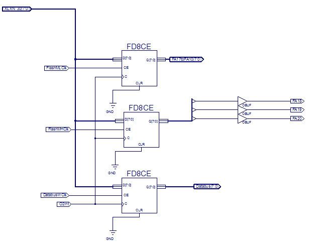
I'm at the point now of presenting the banked address to the Flash, using a 1K window @$0400-$07FF. A simple piece of software I am using to test my circuit is below. $C002 is the LSB and the data can be seen on FA17to10[7:0]. $C004 is the MSB, only the lowest 3 bits are used and can be seen on FA18, FA19, and FA20. I made them readable ports, so I can do a INC/DEC. On to the ISim...
It successfully does an INC but that's it. 1 time only. Also, I don't understand why there are zero's in the IR. Once, right after the INC $C004 (yellow marker), and again after the STX $C002.
Any ideas on either of these?
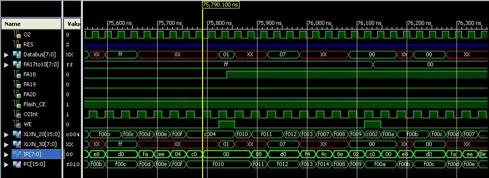
I'm at the point now of presenting the banked address to the Flash, using a 1K window @$0400-$07FF. A simple piece of software I am using to test my circuit is below. $C002 is the LSB and the data can be seen on FA17to10[7:0]. $C004 is the MSB, only the lowest 3 bits are used and can be seen on FA18, FA19, and FA20. I made them readable ports, so I can do a INC/DEC. On to the ISim...
Code: Select all
*= $F000	;4Kx8 ROM


begin      LDY #$07
	        LDX #$00
	        STX $C004
a	       STX $C002
	        INX
	        BNE a
	        INC $C004
	        DEY
	        BNE a
b	       JMP b
Any ideas on either of these?