A 6502 SoC Project using a Spartan 3 FPGA
-
ElEctric_EyE
- Posts: 3260
- Joined: 02 Mar 2009
- Location: OH, USA
I finished wiring the XC3S400 VCCO, VCCAUX, and VCCINT power connections to the GND/POWER bars today. That is, 16 VCCO (incorrectly marked as 12 on the data sheet pg. 140-141) pins, 8 VCCAUX pins 4 VCCINT pins, and 28 GND pins. Also, the 20uF input/10uF output filter cap's for each the VR's, and 1 large 1000uF cap at the 5V in connector.
Long story short, I wound up using what I thought was 26AWG wire wrap wire, instead of the 24AWG as planned... When I tried to strip off the insulation in the clearly stated 26AWG spool in my very clearly labelled auto-wire stripper in the 26AWG slot, it did not strip off the insulator. Fitting the clearly labelled 26AWG wire wrap wire into the 28AWG auto wire stripper cleaned the insulator right off.
I wonder if what I thought I bought as 30AWG is really 32AWG. That spool is unlabelled so I don't really know, unless I get my digital micrometer out, but I suspect it to be so. I will check.
Anyway, tomorrow I wirewrap the FPGA PROM and resistors, JTAG connector and throw the switch.
-
ElEctric_EyE
- Posts: 3260
- Joined: 02 Mar 2009
- Location: OH, USA
I wired all power connections and most of the schematic above, including power to the DS1085L, except the LED, PROGRAM button, and R7.
Very hesitantly switched power on while iMPACT was running and did a boundary scan. Guess what? The smoke came out all over the place! Just kidding, iMPACT saw the XCF02S PROM and the XC3S400 Spartan 3!!!! I may have the courage to leave the power on abit longer now...
Time to power up the scope and check out the anticipated 45MHz (with my 40MHz probes ) out of the DS1085L... No bypass caps yet.
Very hesitantly switched power on while iMPACT was running and did a boundary scan. Guess what? The smoke came out all over the place! Just kidding, iMPACT saw the XCF02S PROM and the XC3S400 Spartan 3!!!! I may have the courage to leave the power on abit longer now...
Time to power up the scope and check out the anticipated 45MHz (with my 40MHz probes
- BigDumbDinosaur
- Posts: 9428
- Joined: 28 May 2009
- Location: Midwestern USA (JB Pritzker’s dystopia)
- Contact:
ElEctric_EyE wrote:
I may have the courage to leave the power on abit longer now...
x86? We ain't got no x86. We don't NEED no stinking x86!
-
ElEctric_EyE
- Posts: 3260
- Joined: 02 Mar 2009
- Location: OH, USA
Thanks BDD!
I observed 45MHz out of the DS1085L...
Wired in the /PROGRAM button.
I'm going to try to get away, for as long as possible, without using bypass cap's. Such a PITA wiring so many...
Next step will be to wire in the 20-pin display connector, finish the schematic, and program the FPGA PROM.
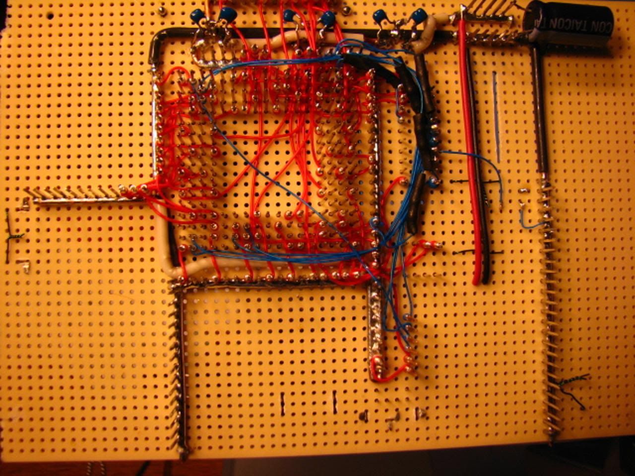
I observed 45MHz out of the DS1085L...
Wired in the /PROGRAM button.
I'm going to try to get away, for as long as possible, without using bypass cap's. Such a PITA wiring so many...
Next step will be to wire in the 20-pin display connector, finish the schematic, and program the FPGA PROM.

-
ElEctric_EyE
- Posts: 3260
- Joined: 02 Mar 2009
- Location: OH, USA
I decided it would be best to take a smaller step to test what I've got so far, by making a simple state machine to initialize the display. A counter, and a ROM to feed the display. Especially since I'm not using bypass cap's. At some point I anticipate problems, but not at this early stage.
There is example code for the display here: http://www.newhavendisplay.com/app_note ... F-CTXI.txt .I am focusing on the "initialize display" portion, very easy. And this display can handle 50MHz Phase 2 (E signal). No problem with the default setting of the I2C controlled DS1085L @45MHz, since there is no I2C controller yet to change the frequency..
This is the same Init routine I'm successfully using on the "proof", i.e. the current 20 MHz PWA project with a WDC65C02, 2Mx8 SRAM, 512Kx8 EEROM, and 100-pin Spartan 2 XC2S50.
I should be able to tackle this before next weekend.
There is example code for the display here: http://www.newhavendisplay.com/app_note ... F-CTXI.txt .I am focusing on the "initialize display" portion, very easy. And this display can handle 50MHz Phase 2 (E signal). No problem with the default setting of the I2C controlled DS1085L @45MHz, since there is no I2C controller yet to change the frequency..
This is the same Init routine I'm successfully using on the "proof", i.e. the current 20 MHz PWA project with a WDC65C02, 2Mx8 SRAM, 512Kx8 EEROM, and 100-pin Spartan 2 XC2S50.
Code: Select all
   LDA #$01	;software reset
	STA dcom
	STA dcom
	STA dcom

	LDX #$ff	;delay
a	DEX
	BNE a

	LDA #$e0	;start PLL
	STA dcom
	LDA #$01
	STA ddat

	LDX #$ff	;delay
b	DEX
	BNE b

	LDA #$e0	;lock PLL
	STA dcom
	LDA #$03
	STA ddat

	LDA #$b0	;set LCD mode, 640x480
	STA dcom
	LDA #$0c
	STA ddat
	LDA #$80
	STA ddat
	LDA #$02
	STA ddat
	LDA #$7f
	STA ddat
	LDA #$01
	STA ddat
	LDA #$df
	STA ddat
	STZ ddat

	LDA #$f0	;set interface format:8-bit
	STA dcom
	LDA #$00
	STA ddat

	LDA #$3a	;set RGB format, 18 bits per pixel
	STA dcom
	LDA #$60
	STA ddat

	LDA #$e6	;set pixel clock
	STA dcom
	LDA #$04
	STA ddat
	LDA #$ff
	STA ddat
	LDA #$ff
	STA ddat

	LDA #$b4	;set Horizontal Period
	STA dcom
	LDA #$02
	STA ddat
	LDA #$f8
	STA ddat
	STZ ddat
	LDA #$44
	STA ddat
	LDA #$0f
	STA ddat
	STZ ddat
	STZ ddat
	STZ ddat

	LDA #$b6	;set Vertical Period
	STA dcom
	LDA #$01
	STA ddat
	LDA #$f8
	STA ddat
	STZ ddat
	LDA #$13
	STA ddat
	LDA #$07
	STA ddat
	STZ ddat
STZ ddat-
ElEctric_EyE
- Posts: 3260
- Joined: 02 Mar 2009
- Location: OH, USA
Following the previous idea to it's conclusion led me to realize I would need 3 ROMs. 1 for each address (ddat and dcom) and a controller ROM, to enable either of the address ROM's. Also, a couple counters...
At this point, I realized I need to just go ahead with implementing Arlet's core with the internal RAM and ROM. It's seems simpler from a schematic point of view...
_______________________________________________________________
EDIT (2/21/11) It just occurred to me to use a 40bx9 ROM and use the 9th bit as the address select. I will have to look at the timing requirements, as I am sure the data will have to be delayed through a register with respect to the address...
-
ElEctric_EyE
- Posts: 3260
- Joined: 02 Mar 2009
- Location: OH, USA
Got the internal schematic completed this morning and it passed synthesis with just a few warnings. The O2 (phase 2), RES, and RES2 are the only inputs so far. Databus(7:0), A0, R/W,and /Display are the only outputs and will be wired to the 640x480 TFT display.
I've used no constraints so far, and after looking at the Timing Constraints in the Design Summary after synthesis, the design is auto time spec'd @20ns. Maybe it will run @45MHz right off the bat.
Time to wire in the display connector to the FPGA. Then I have to rewrite the software for the original 6502. And then I will be on to some serious troubleshooting methinks...
Also, I have to find out how to change the I/O standard to LVCMOS3.3v. Right now ISE is setting the default to LVCMOS2.5v.
EDIT: Figured out IOStandard. Had to modify the .vf file ISE makes after synthesizing the top-level schematic, by changing "default" to "LVCMOS33".
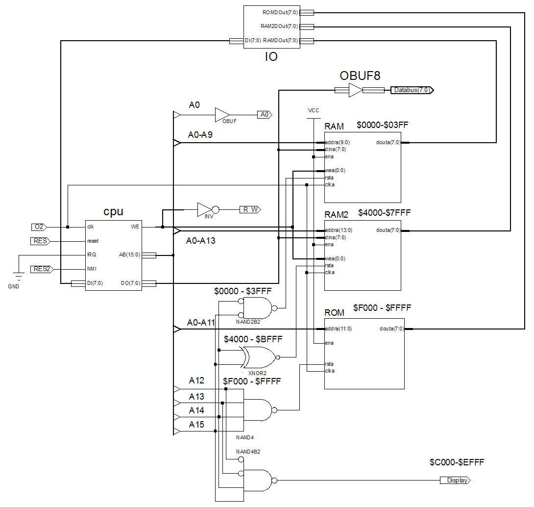
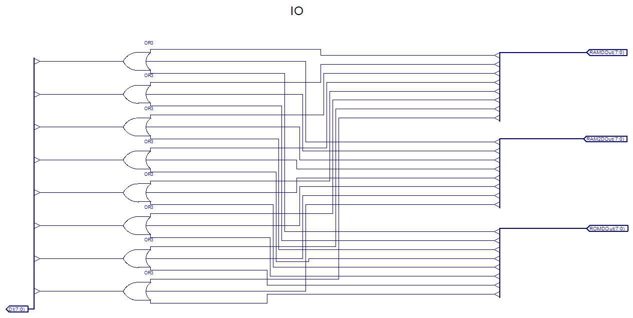
Inside the IO symbol above (it is rotated and mirrored so the inputs/outputs appear skewed):
I've used no constraints so far, and after looking at the Timing Constraints in the Design Summary after synthesis, the design is auto time spec'd @20ns. Maybe it will run @45MHz right off the bat.
Time to wire in the display connector to the FPGA. Then I have to rewrite the software for the original 6502. And then I will be on to some serious troubleshooting methinks...
Also, I have to find out how to change the I/O standard to LVCMOS3.3v. Right now ISE is setting the default to LVCMOS2.5v.
EDIT: Figured out IOStandard. Had to modify the .vf file ISE makes after synthesizing the top-level schematic, by changing "default" to "LVCMOS33".

Inside the IO symbol above (it is rotated and mirrored so the inputs/outputs appear skewed):

ElEctric_EyE wrote:
Also, I have to find out how to change the I/O standard to LVCMOS3.3v. Right now ISE is setting the default to LVCMOS2.5v.
EDIT: Figured out IOStandard. Had to modify the .vf file ISE makes after synthesizing the top-level schematic, by changing "default" to "LVCMOS33".
EDIT: Figured out IOStandard. Had to modify the .vf file ISE makes after synthesizing the top-level schematic, by changing "default" to "LVCMOS33".
There's also something like 'Create Timing Constraints', where you can add a simple timing constraint for the clock input.
The user constraints are stored in a .ucf file, which you can also edit in your favorite text editor.
-
ElEctric_EyE
- Posts: 3260
- Joined: 02 Mar 2009
- Location: OH, USA
Before you replied (thanks for being so quick), I did abit more reading and started using PlanAhead which is part of the Xilinx software bundle. I was able to finally use it to make a txt based .ucf constraints file which allowed me to manually assign each of the outputs for LVCMOS33.
In 12.3, the constraints editor is under the Tools menu, and I didn't see anything for setting IOStandard, I checked and rechecked and rechecked...
So now I've just finished wiring the display connections and reattached the display to the board. After a short rest, as my back is killing me, I will rewrite the display init routine and try to program the PROM. (In my younger days I would've been obsessed by this and been done in a few days! I would've made more mistakes though...)
I just checked out ISE 12.4, and followed 'User Constraints' in the Processes window, then clicked on 'I/O Pin Planning (PlanAhead) - Pre-Synthesis'.
This opens the PlanAhead tool, in this tool there are several windows, on the top left is the design, and somewhat lower is the 'Package Pins' window.
On the design, choose the "I/O Ports tab", and this should show all your I/O ports, and for each port you can choose a "Site" (pin number), I/O standard, and some other options. Note that this window is too narrow to show all the columns. You'll have to make it wider, or use the scroll bar.
You can also go to the 'Package Pins' window, and open up a bank. Now you can click on a I/O port in your design, and drag it into the appropriate row in the Package Pins.
-
ElEctric_EyE
- Posts: 3260
- Joined: 02 Mar 2009
- Location: OH, USA
Right, that worked...
Got the voltage levels correct, locked the pin assignments. Wired the display connector. Rewrote the display init, and clearscreen routines for original 6502. Assembled it, and saved the file as a binary image (.65b). Renamed it to .bin. Opened it up in a hex editor and added the reset vector. Converted the .bin to a .coe file with your .coe converter (version 2). Went back into ISE and updated the ROM using Block Generator. Successfully resynthesized everything and generated the .bit program file. Powered up the 6502SoC and went into ISE iMPACT and successfully programmed the PROM using the PROM file formatter. iMPACT sees the PROM and FPGA and I can read device codes from both, also blank checked the PROM, and it is not blank.
So my JTAG interface seems reliable, however nothing is happening when I push the /PROGRAM button. No clock signal out of the FPGA (pin 3 of the PROM). I realize I still have not put in an R7 (pg.6), which may prevent the circuit from 100% functioning, but I think I should still see some kind of clock signal. Will check my wiring.
WOOPS, found 47K resistors. Should be 4.7K. I need better lighting! Forgot to wire the mode pins and hswap pin. Now getting 6MHz out of the FPGA for a sec after powerup, and when pressing /PROGRAM button.
Reread the configuration section on the datasheet and changed a few things to comply...
PROM voltages on PG. 8 of XAPP453 and Pg. 47 the Spartan 3 datasheet are not jiving... Going to be trial and error
-
ElEctric_EyE
- Posts: 3260
- Joined: 02 Mar 2009
- Location: OH, USA
HOORAY HOORAY HOORAY!!!!!! Success!
Initially I saw constant activity on the databus. When I hit the /PROGRAM button, the display's /CS line would go low for 3 times then stop. Looked like something was crashing, so I divided the Phase 2 internally down to 10MHz and brought it out to the display and bam! It worked!
I think the display is the limiting factor. There are 2 software delays present in the init routine. Could be it's not getting enough time running @45MHz. I think the core is running fine @45MHz as evidenced by the active databus. I will try lengthening the delays.
I will post an updated schematic of the JTAG interface soon. Now the fun begins!
After a few more tests (Down to 2.8MHz right now), I can say the display is getting data and the screen is clearing. But when I try to INC the 3 color variables, which are stored in zero page, in a simple loop, the colors are not changing. I do a JSR to the CLRSCR routine within the loop and it appears to be running smooth, meaning the data stored in the stack for the JSR/RTS is being written/read successfully. Also, the reset is not working, it locks the system up. So not everything is perfect yet. I think I will start a new project file and re-input everything fresh, even though this version of ISE seems much more stable than earlier versions.
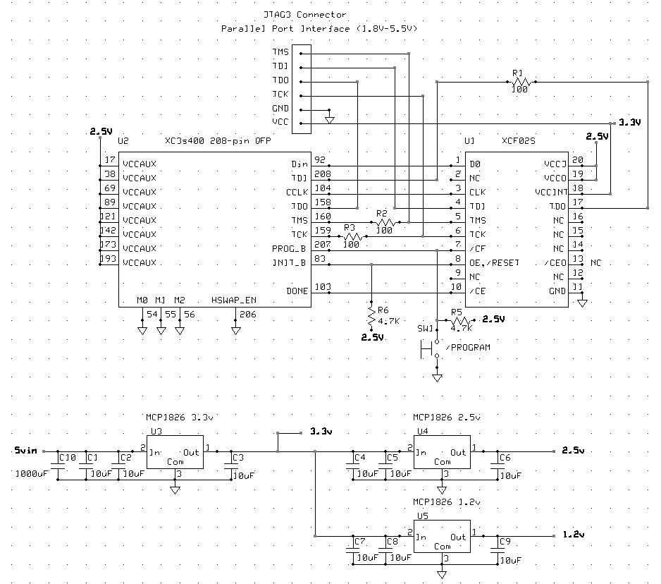
This is what I have for the JTAG interface.

-
ElEctric_EyE
- Posts: 3260
- Joined: 02 Mar 2009
- Location: OH, USA
Re-inputting fresh data into a new project file changed nothing. The circuit behaved exactly the same, which is a credit to Xilinx software dep't. This was not so in ISE 10 & 11. Sometimes performing a "cleanup project files" would drastically change performance. The only beef I have at this point is the software is not backwards compatible with some of the earlier Xilinx families like Spartan 2, even though they still are selling very well and are very much alive...
I've had experiences with random/wrong data in other projects. This problem with totally wrong data but a good /CS for the display led me to believe the O2 is skewed, because the display is external and the FPGA internals (CPU/RAMs/ROM) appear to be working. O2 is most likely skewed internally as well, from the CPU to the RAM's & ROM, but to a much smaller degree and most likely will not be noticeable until higher O2 speeds are used. Proof of this suspicion is I inverted O2 to the display and it was receiving correct data. Screen was clearing from black to white @2.8 MHz. Not ready to test at higher speeds yet. Time to get some experience with the DCM's coarse & fine phase shift abilities now that I have zeroed in on the problem.
Some other observations:
1) The "massive" heat sink on the VR's is very cool to the touch, granted running at a slow speed but still extreme overkill I think. Still, I have expansion slots to add later...
2) The /PROGRAM button is not 100%. To get the FPGA running reliably in a continuous loop requires several pressings.
-
ElEctric_EyE
- Posts: 3260
- Joined: 02 Mar 2009
- Location: OH, USA