6502.org Forum  Projects  Code  Documents  Tools  Forum
It is currently Sun Nov 10, 2024 7:35 pm

All times are UTC


Post new topic Reply to topic  [ 63 posts ]  Go to page Previous  1, 2, 3, 4, 5  Next
Author Message
 Post subject:
PostPosted: Sat Oct 30, 2010 10:39 pm 
Offline
User avatar

Joined: Thu Dec 11, 2008 1:28 pm
Posts: 10976
Location: England
RichTW wrote:
BigEd wrote:
The tcstate presentation is a bug, I'm afraid. It should show values like 011111, 101111 and so on, but I added the bits instead of concatenating them. There's a fix in the works!

That's great! I'll hang on for the next release :) I'm intrigued by the tcstate - it doesn't seem to be quite as straightforward as it was originally made out to be.

Glad to tell you that the new (pre)release was made earlier today. It's much faster and the tcstate presentation is now right. Also the predecode register was reported inverted. (Now it's the right way up, but masked in most cycles by the clearIR signal. Ah well.)

An example URL for the pre-release area is:
http://visual6502.org/JSSim/expert.html ... loglevel=5
[Edit - now released!]
As this lands on the 'expert' page you may need to know that the layout view responds to '>' and '<' for zooming, drag to pan and click to select a signal.

(Credit to the whole visual6502 team, of course: I'm only announcing!)

Cheers
Ed


Top
 Profile  
Reply with quote  
 Post subject:
PostPosted: Thu Nov 11, 2010 10:20 pm 
Offline

Joined: Thu Nov 11, 2010 10:14 pm
Posts: 9
Hi all.
I maintain the T65 core (www.fpgaarcade.com) which is (so I'm told) one of the more accurate VHDL implementations.

As an ASIC designer, I have to say this visual6502 is an amazing piece of work - congratulations to all involved.

I also have to say I never thought I would see a javascript chip emulator!

I'm interested in taking the netlist and converting it back into a VHDL model we can run in the FPGAs, and I've started work on this. It is partly automatic, but there will be a fair amount of tweaking to get it map efficiently to FPGA architecture.

I'm trying to get the software to identify groups of transistors and replace them with a flop for example.

Any news on other netlists??? :)

Best,
MikeJ
www.fpgaarcade.com


Top
 Profile  
Reply with quote  
 Post subject:
PostPosted: Fri Nov 12, 2010 11:02 am 
Offline

Joined: Mon Mar 02, 2009 7:27 pm
Posts: 3258
Location: NC, USA
Welcome Mike! :shock: :D

_________________
65Org16:https://github.com/ElEctric-EyE/verilog-6502


Top
 Profile  
Reply with quote  
 Post subject:
PostPosted: Sun Nov 14, 2010 2:27 pm 
Offline
User avatar

Joined: Thu Dec 11, 2008 1:28 pm
Posts: 10976
Location: England
Hi Mike
good to see you here! T65 is very nice, glad to hear that you're looking after it.

It is amazing that Javascript is capable of switch-level simulation at useful speeds - useful for education purposes anyway.

I think there's a 6800 netlist somewhere in the pipeline, but I don't know when it might reach the open air. It will be very interesting to compare.

As for FPGA modelling, you're not the only one interested! Brian and Barry, the authors of the javascript simulation model, are quite keen on keeping it general purpose and not assuming too much. There's no reason why others might not step up and implement something at logic gate level, but they'd have to tackle the wide use of pass transistors: for storage, for multiplexing, for bus drivers and for coupling busses together. There's an idea that there are only two sets of pass transistors on 6502 which are genuinely bidirectional, but I don't think there is yet proof of that. One approach is to try to model the 6502 and another approach is to apply some general-purpose transformations which would map any similar netlist to working HDL. (See Donald Hanson's paper)

I'll be interested to hear about your progress, and maybe I can help in some way.

Cheers
Ed


Top
 Profile  
Reply with quote  
 Post subject:
PostPosted: Sun Nov 14, 2010 7:06 pm 
Offline

Joined: Thu Nov 11, 2010 10:14 pm
Posts: 9
Thanks Ed.

I've got quite a bit of experience going from net lists (or GDS files) back to VHDL, I've been working on some Atari ST chip for a while.

For chips which were built from a standard cell library it's quite a bit easier as you can identify the groups of transistor in the cell and replace those with a logical equivalent. I've build up a library of such models.

I've written a c++ program which is nice and generic so far. It reads in the trans, segs and node name files and dumps out a netlist with instantiated models for the transistors and pull ups etc.

It needs a bit of hand hacking to bring the right nets to the IO, but I am quite close to being able to simulate it. Do you have a test suite I can use by the way?

Assuming my extraction is ok, I can then use LEC (conformal) testing using this model as a baseline against modified code.

The next step is to trace the clock nets and find and replace flops.

For the pass transistors the model is bi-directional at the moment. I should be able to work out where the net drivers are and reduce the logic.
I may throw the whole thing at a synthesis tool (synplicity) and get it to work out what's going on. The tools can be used to write out an optimized VHDL file I can then hand hack.

Which pass transistors are suspected to be bi-directional at the moment?

I'll keep you informed of progress. I've got a lot to do at the moment so I don't know how long it will take.
Cheers,
Mike


Top
 Profile  
Reply with quote  
 Post subject:
PostPosted: Sun Nov 14, 2010 7:19 pm 
Offline
User avatar

Joined: Thu Dec 11, 2008 1:28 pm
Posts: 10976
Location: England
Hi Mike
having access to (expensive) formal comparison tools is a big help!

In Hanson's 6502 block diagram we see two blocks of "pass mosfets" which couple the SB (special bus) to two other busses. These 16 pass transistors are thought to be the only ones which act bidirectionally - as determined by examining all transistors, not by taking the diagram as primary. (In fact Hanson had access to original 6502 blueprints.)

For a testsuite, I most recently used a slightly modified version of the test ROM from the hmc-6502 project. There's a thread about testsuiteswhich would be a good place to collect wisdom. I gather from some fault-analysis type of simulations that booting C64 basic only exercises about 2/3rds of the transistors, which is a bit surprising.

Cheers
Ed


Top
 Profile  
Reply with quote  
 Post subject:
PostPosted: Sun Nov 14, 2010 7:43 pm 
Offline

Joined: Thu Nov 11, 2010 10:14 pm
Posts: 9
Thanks for the pointers Ed,

Having access to the professional tools does help, one of the advantages of working at a company which designs ASICs :)

Even though I work more with FPGAs than the ASICs nowadays I try and drive the layout tools occasionally otherwise I forget everything pretty fast.

I know quite a few guys who did layout work in the late 80's early 90's and a lot of them have bits and pieces of documentation still which was really useful in analysing some other chips.

I mailed the guys who did the C64 SID die scans a while back, they were stuck at the vectorisation stage.

http://mail.lipsia.de/~enigma/neu/6581.html
http://oms.wmhost.com/misc/

If you have developed some semi-automatic vectorisation techniques it may be work chatting to them.

We have layout vs schematic tool, and part of this is being able to create a netlist from a GDS file. However, getting it to work from raw polygons was difficult.
Best,
Mike


Top
 Profile  
Reply with quote  
 Post subject:
PostPosted: Sun Nov 14, 2010 9:12 pm 
Offline
User avatar

Joined: Thu Dec 11, 2008 1:28 pm
Posts: 10976
Location: England
Hi Mike
thanks for pointing out all that SID work - I'll look into that. I'm a bit pessimistic about being able to reverse engineer from photos alone, if the design isn't strongly cell-based. That is, a custom design may need some deprocessing so we can see beneath the metal. Unless we're lucky.

For vectorisation, I think 'semi-automatic' is as good as it gets, but there's some action on tool-building so with luck we'll be in a position to help before too long.

For simulation, other than Hanson's approach, there's also this paper:
COSMOS: A Compiled Simulator for MOS Circuits, Randal E. Bryant & co
and even some source (which I wasn't able to compile - maybe you'll be better equipped.)

Cheers
Ed


Top
 Profile  
Reply with quote  
 Post subject:
PostPosted: Mon Nov 15, 2010 6:28 pm 
Offline

Joined: Mon Nov 15, 2010 6:05 pm
Posts: 1
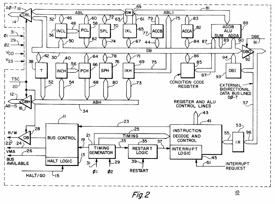
First of all: this is an amazing project. All my congratulations. Concerning the 6800, I found a patent which explains some of the internals of this processor. Have a look for patent 4090236 (e.g. http://www.freepatentsonline.com/4090236.pdf)
Do you think it would be possible to create a readable schematic diagram from the netlists?


Top
 Profile  
Reply with quote  
 Post subject:
PostPosted: Mon Nov 15, 2010 6:39 pm 
Offline
User avatar

Joined: Thu Dec 11, 2008 1:28 pm
Posts: 10976
Location: England
Hi - thanks for the pointer to that patent! They are often interesting but not always easy to find. I've uploaded the 6800 block diagram - see below.

We'd like to construct a schematic, and ideally animate it. We might be able to adapt Balazs' giant schematic - there are a few errors and also maybe differences between the two chips. (See 4004.com for some animated schematics.) I'm thinking it's more a question of writing a program to compare the schematic with the layout, and correct the schematic, not a process of deriving schematics from the layout. But I might be wrong about which approach is more practical.

Cheers
Ed

Image


Last edited by BigEd on Sun Oct 04, 2015 3:58 pm, edited 1 time in total.

Top
 Profile  
Reply with quote  
 Post subject:
PostPosted: Tue Nov 16, 2010 2:19 am 
Offline

Joined: Tue Nov 16, 2010 2:07 am
Posts: 16
Wow, fantastic work. Many thanks.

But why the netlist and/or the die image is not public? I realize you don't have a "standard" SPICE, or Verilog netlist. But the netlist in whatever format would be nice to have. What about the die image matrix?

BigEd wrote:
... interested in the 6800, because I'd like to see what similarities and differences exist ... And the answer is...
much less than I expected! I'm shocked!


Actually the difference is expected (or you meant that they loook rather similar?). MOS intentionally made a design from scratch, they knew that otherwise they would be in legal troubles (more than what they eventually were). Also, the original 6800 was enhancement load, not depletion load like the 6502.


Last edited by ijor on Tue Nov 16, 2010 2:31 am, edited 1 time in total.

Top
 Profile  
Reply with quote  
 Post subject:
PostPosted: Tue Nov 16, 2010 2:28 am 
Offline

Joined: Tue Nov 16, 2010 2:07 am
Posts: 16
fpgaarcade wrote:
For chips which were built from a standard cell library it's quite a bit easier as you can identify the groups of transistor in the cell and replace those with a logical equivalent. I've build up a library of such models.


Hi Mike. You might know better than me, but I don't think there was such thing as standard cell library in NMOS chips. Certainly not in these older ones where the layout was done manually.

BigEd wrote:
...Balazs' giant schematic - there are a few errors and also maybe differences between the two chips.


Yeah, there are some obvious, and some not so obvious errors. I think that he run out of time, and his main point was more a proof of concept anyway.


Top
 Profile  
Reply with quote  
 Post subject:
PostPosted: Tue Nov 16, 2010 10:37 am 
Offline

Joined: Thu Nov 11, 2010 10:14 pm
Posts: 9
Hi Ijor,

Certainly there were no standard libraries used for the very early chips. For the later ones (Atari ST/Amiga days) they were built using standard cells.

The libraries were specific to the gate array being used for that project, but at least all the 2 input and gates look the same throughout the design for example.

For the 6502 it was all done by hand I believe, so every transistor counted.

Best,
Mike


Top
 Profile  
Reply with quote  
 Post subject:
PostPosted: Thu Nov 18, 2010 7:32 am 
Offline
User avatar

Joined: Thu Dec 11, 2008 1:28 pm
Posts: 10976
Location: England
Hi Ijor
I see elsewhere that you have photos of the ANTIC chip. It'll be interesting to see what can be made of that!

Greg has some tools to assist in capturing layout from photos, and also there's degate.

Greg's tools, like his die photos, are not quite released yet but I believe the plan is to make them available. Please be patient!

As for the visual6502 netlist, it's captured and *relatively plainly tabulated in the javascript. It shouldn't be too hard to translate it into a different form. But because it's at transistor level, and because there are bidirectional pass gates, you'd need the right kind of simulator. SPICE would do it - would it be usefully fast? It might be too low level: the gate lengths would need to be sized, and that information is not present in the javascript. I don't know about verilog (and therefore about FPGA) - if you have good ideas about modelling bidirectional pass gates then we can try it. (Send me a PM.) Not sure about the MAGIC tools - again, if you want to have a go, I'll try to help. It would be great if someone could get the COSMOS simulator built and running. Switch level simulation used to be a hot topic.

There are many possible ways forward... should be interesting.

Cheers
Ed

* all the connectivity for pulldowns and the enhancement(**) pullups are in transdefs.js, but the depletion pullups are in segdefs.h together with the layout-derived polygons. There's also nodenames.js for the naming.

* COSMOS: A Compiled Simulator for MOS Circuits, Randal E. Bryant & co

(**) Edit: oops, I've been misunderstanding the use of depletion versus enhancement pullups. Probably the vast majority are depletion mode: we can't actually tell from the photos.

Last edited by BigEd on Mon Nov 22, 2010 8:00 pm, edited 1 time in total.

Top
 Profile  
Reply with quote  
 Post subject:
PostPosted: Thu Nov 18, 2010 1:23 pm 
Offline

Joined: Thu Sep 02, 2010 12:34 am
Posts: 36
Location: Salzburg, Austria
Hi Ed!

BigEd wrote:
For simulation, other than Hanson's approach, there's also this paper:
COSMOS: A Compiled Simulator for MOS Circuits, Randal E. Bryant & co
and even some source (which I wasn't able to compile - maybe you'll be better equipped.

The link to the source code doesn't work (for me). 2 days ago I got a 404, yesterday and today it's a 500. I even started my XP VM with IE, but still no luck :-(

Do you have a copy of the source code and, if yes, could you send it to me? I'll then have a look at the code, the paper sounds interesting.

so long,

Hias


Top
 Profile  
Reply with quote  
Display posts from previous:  Sort by  
Post new topic Reply to topic  [ 63 posts ]  Go to page Previous  1, 2, 3, 4, 5  Next

All times are UTC


Who is online

Users browsing this forum: No registered users and 1 guest


You cannot post new topics in this forum
You cannot reply to topics in this forum
You cannot edit your posts in this forum
You cannot delete your posts in this forum
You cannot post attachments in this forum

Search for:
Jump to: