Cycle stretching is definately worth looking into, so I'll pose just a few more questions...
So if I am having success reading an EEPROM at a certain MAX 50/50 Phase 2 speed, could I surpass this speed using 75%/25% cycle stretching?
How would the type of address decoding (i.e R/W with Phase2, or Address with Phase 2) be affected by cycle stretching?
EDIT: Reclarified question(s).
Project: Digital Fuel Injector Pulse Width Analyzer
-
ElEctric_EyE
- Posts: 3260
- Joined: 02 Mar 2009
- Location: OH, USA
Last edited by ElEctric_EyE on Sat Sep 25, 2010 9:27 pm, edited 1 time in total.
-
BigDumbDinosaur

- Posts: 9428
- Joined: 28 May 2009
- Location: Midwestern USA (JB Pritzker’s dystopia)
- Contact:
Re: RDY Generation
kc5tja wrote:
BigDumbDinosaur wrote:
It would seem executing WAI with this circuit would result in the MPU trying to sink the output of that last OR gate when it's high (no wait-state wanted).
Quote:
I mentioned earlier (in another thread? I can't remember) that you're expected to drive RDY through a (IIRC, 470 ohm) resistor at the CPU pin. I didn't show the resistor here because it's needless detail, and if you have multiple sources of RDY generation, it doesn't make any sense to put it here anyway.
I'm not trying to castigate you in any way, but a lot of folks pass through here looking for technical info, many of whom may not be as expert as you or other regulars when it comes to this sort of stuff. Including what we might think of as obvious circuit features helps the folks who maybe want to rig up their own 65xx contrivance to avoid making design errors that can cost them time and money in blown up parts.
x86? We ain't got no x86. We don't NEED no stinking x86!
-
ElEctric_EyE
- Posts: 3260
- Joined: 02 Mar 2009
- Location: OH, USA
BDD I see you your point. I used to blow out IC's when I was young. But even back then I was able to read data sheets. If anyone just starts connecting pins without regard to manufacturer spec's, then they should expect to see the "smoke go out" at some point...
I'm concentrating right now on address decoding logic. As I said previously, my intent is to copy any portion of a 512Kx8 EEPROM to anywhere within a 2Mx8 SRAM with software, control phase 2 speeds with a software programmable 1-bit port, and run the OS from SRAM at hopefully @ 14+MHz. Initial tests indicated 20MHz was successful while observing SYNC with a simple delay loop.
Although memory decoding was incorrect and SRAM was only active between $0C000-$0FFFF, the loop was running successfully, and delays were changing as expected. I was not using zero page or stack. The delay variable was in the Y register...
Last night I was able to run the display init routine from anywhere within the CPU's 64K using EEPROM only. Except for addresses $00000-$001FF & $08000-$0BFFF (zero page, stack and I/O). I think I have the /CE's correct.
Next step is correcting the /OE decoding logic for the SRAM/EEPROM. Tomorrow I will have dedicated time to iron it out.
I need to update my memory map from a few pages ago.
Next I will attempt to interface to a mini PS2 keyboard using Daryl's interface with an Atmel ATTiny 24.
EDIT:
SUCCESS! on the morn of 9/27/2010.
I'll skip all the irrelevant, improper address decoding techniques I was using, and get right to the "solid food".
I was using an FDCE "D" type flip-flop inside the Spartan 2 for the Phase 2 control bit. This flip-flop controls what the WDC65C02 sees on the O2In and simultaneously controls the SRAM_OE and EEPROM_OE's in conjunction with a $00000-$0001FF address decode. After ramping up the "higher" speed for Phase 2 from 5MHz to 20MHz, I would notice the speed, at a random time would switch back down to 2.5MHz. Meaning D0 was being latched right on the edge, incorrectly. I knew it was a speed issue as this did not happen when the "higher" speed was set to 10MHz...
Switching to an IFDX "D" type flip-flop, (which is the same type of flip flop, without a reset, except that it is internally connected to input pads (pins), namely Phase2, D0, and an address decode), is working very reliably now running more than 30 minutes at 20MHz.
Once I learn to clear display I will make a small video on Utube. Right now I am unsure why I am addressing a small window in the display. Within the window, the software loop is displaying the correct data, nothing random @ 20 MHz.
-
ElEctric_EyE
- Posts: 3260
- Joined: 02 Mar 2009
- Location: OH, USA
I found out why I was addressing a small window, instead of the entire 640x480 display. Apparently an STZ to display registers is not sending correct data. Although the data is consistent it was not a zero value. I found this out this morning before heading to work. I was experimenting with the display init values and decided before changing some values, that I would rewrite the code to do an LDA, STA to make it easier to just change a few values. SO starting with LDA #$00, STA displaydata, instead of STZ displaydata, it worked! as it should have from the beginning?... I know it's not a speed issue, as I've tried running from SRAM down to 2.5MHz (same as EEPROM copy speed) and have seen the same result.
So although I m pleased with this progress, I seem to be regularly making 2 steps forward, 1 step backward (sometimes even 1 step foward, 2 steps backward)...
Also I have learned alot about using symbols in the Xilinx ISE 10.1. It was about a 2 week struggle to get my custom symbols (symbols=schematic reduction)to work like the original schematic without symbols. Symbols in ISE are chunks of a main schematic, similar to making your own custom IC. I found it necessary because my original single schematic was growing beyond the limits of ISE's largest setting. Initially, I divided it into 3 symbols. 1 for memory decoding , 1 for banked address decoding, and 1 for the phase 2 switching circuit. Made sense to me, but not so easy... ISE 10.1 software was optimizing out my memory decode symbol. It saw bank address decode as priority, and negated wherever else the Address bus went. I realized this after synthesis errors... After combining the address decode and bank address symbols into 1 symbol, which both use A8-A15, the circuit worked as the original... I'm still learning. Maybe one day I learn VHDL.
Anyway, I once again have a working circuit within the FPGA with the W65C02 running @20MHz. My address decoding is still leaving alot to be desired...
Which is why I am posting tonight... System runs great until I hardware reset. It's a SRAM bank issue, it's ok. Now I've made it this far I want to strive for something ever better...
In my original idea, I wanted the address decode to switch down to the lowest 16K block inside the 2Mx8 SRAM ($000000-$0001FF) when zero page or stack was seen on the address bus (A0-A20) for the lower 16K block, and to switch to the highest 16K block for where the OS resides $1FC000-$1FFFFF.
Now I am thinking of 32K memory blocks with current zero page/stack memory spread across every 32K block within the 2M SRAM. So when I switch 32K memory banks $xx0000-$xx7FFF, zero page /stack is retained. Is it even possible to rewrite multiple chunks of memory simultaneously? This way, bank switching in between a 32K copy using Indirect-Indexed would be successful.
Last edited by ElEctric_EyE on Fri Oct 08, 2010 3:55 am, edited 3 times in total.
-
ElEctric_EyE
- Posts: 3260
- Joined: 02 Mar 2009
- Location: OH, USA
-
GARTHWILSON

- Forum Moderator
- Posts: 8775
- Joined: 30 Aug 2002
- Location: Southern California
- Contact:
It sounds like you have a 65CE02 and got something else in the Z register, so when you do STZ, you get something other than 0. The 65CE02's Z register is initialized to 0 upon reset, but you can store other values in it, IIRC. But on the 65c02, I have never had trouble with STZ. It has always stored 0.
An individual SRAM chip won't let you write to more than one address at a time. Why not have your CPLD divide up the SRAM in 64 32KB sections, and have the lowest one alway be addressable regardless of which section is being pointed to by the CPLD for the other part of your 64KB address map. You need more than just ZP and page 1 to remain common, for reasons of variables and having code that stays in control when you switch the banking. You'll have more useful space because you won't have redundant sections of RAM. If I misunderstood you, just disregard.
An individual SRAM chip won't let you write to more than one address at a time. Why not have your CPLD divide up the SRAM in 64 32KB sections, and have the lowest one alway be addressable regardless of which section is being pointed to by the CPLD for the other part of your 64KB address map. You need more than just ZP and page 1 to remain common, for reasons of variables and having code that stays in control when you switch the banking. You'll have more useful space because you won't have redundant sections of RAM. If I misunderstood you, just disregard.
-
ElEctric_EyE
- Posts: 3260
- Joined: 02 Mar 2009
- Location: OH, USA
-
GARTHWILSON
- Forum Moderator
- Posts: 8775
- Joined: 30 Aug 2002
- Location: Southern California
- Contact:
-
ElEctric_EyE
- Posts: 3260
- Joined: 02 Mar 2009
- Location: OH, USA
I know you're right Garth, about the '816 being more capable than the '02. That's a whole other chapter though...
For now, I stick with the W65C02 PLCC. I've made alot of changes since the original design, and I plan to follow through to completion on this PWA project with the current ideas around the 6502. I've made so many mods since the original post on this thread, with the intent to make a "foundation" for future projects...
ISE being a PITA again, I'll update next week.
WDC needs to put the '816 or the '02 in a QFP package and see which one sells more... Maybe, put them BOTH in QFP, a limited run maybe. I'd buy a heck of alot of '02's, maybe some '816's in the QFP style package.
-
ElEctric_EyE
- Posts: 3260
- Joined: 02 Mar 2009
- Location: OH, USA
Tomorrow I make the video of my 4 IC masterpiece:
1 2Mx8 10nS SRAM
1 512Kx8 200nS EEPROM
1 WDC65C02
1 Spartan 2 FPGA
6502 Phase 2 speed is dynamically switchable via a software programmable "speed bit" to facilitate on the fly copying from EEPROM to SRAM without CPU reset.
2.5MHz when reading from the 200nS EEPROM. 20MHz when system runs from SRAM.
3.3V operation only, however Spartan 2 has 5V input tolerance.
ElEctric_EyE wrote:
Tomorrow I make the video of my 4 IC masterpiece:
1 2Mx8 10nS SRAM
1 512Kx8 200nS EEPROM
1 WDC65C02
1 Spartan 2 FPGA
1 2Mx8 10nS SRAM
1 512Kx8 200nS EEPROM
1 WDC65C02
1 Spartan 2 FPGA
I imagine the Spartan2 to be much more powerful, right? Or is it the speed?
André
-
ElEctric_EyE
- Posts: 3260
- Joined: 02 Mar 2009
- Location: OH, USA
Andre, I chose the FPGA because I wasn't 100% sure my bank switching scheme would work. I had envisioned a worst case scenario where I would've had to put zero page and stack in an internal synchronous ram inside the FPGA. The bank switching works, and now I have alot of room to work with. Alot more potential!
Working with CPLD's, I'm sure you've noticed how quickly a MUX will use up CPLD resources. I've used a 16 to 1 MUX on an XC9572 44-pin PLCC in my old design. Just the 1 MUX used over 50% of resources! Not so in an FPGA... However, on the flipside in my very limited experience, it was much easier to design a tri-state bidirectional bus with a CPLD. Quite a PITA with the FPGA! But 16-bit MUX's & 16-bit identity comparators and more will fit easily into this "smaller" version of the Spartan 2. I don't currently use them in my design, but I have tested them...
I spent a good portion of today making a video of my new hardware build. It was much easier than last year when I had first posted videos on youtube. This new one is a blurry silent movie, but still worth watching as I have annotations for all that is going on.
http://www.youtube.com/ultimateroadwarrior9
Now my brain is having to be switched into software mode! I am done with the hardware for awhile, till I figure out how to correctly send 3 8-bit data in a loop. 256/3 is not an integer... Any pointers?
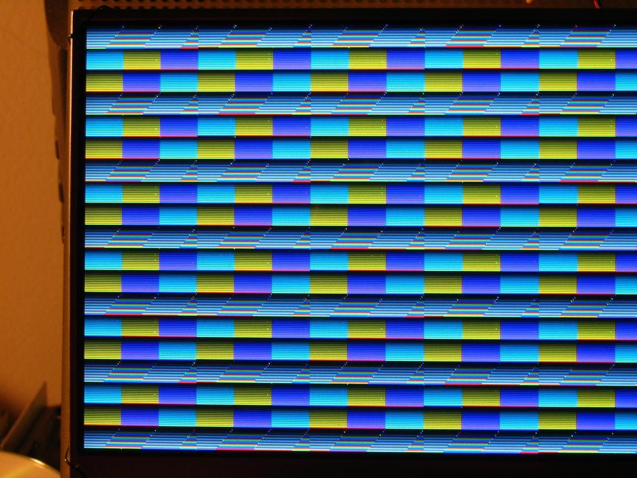
Here's a clearer pic of what I've got so far. SRAM is reliably being written to and read from @20MHz and sent to the display, but not as desired. I'll post the software loop tomorrow:
Working with CPLD's, I'm sure you've noticed how quickly a MUX will use up CPLD resources. I've used a 16 to 1 MUX on an XC9572 44-pin PLCC in my old design. Just the 1 MUX used over 50% of resources! Not so in an FPGA... However, on the flipside in my very limited experience, it was much easier to design a tri-state bidirectional bus with a CPLD. Quite a PITA with the FPGA! But 16-bit MUX's & 16-bit identity comparators and more will fit easily into this "smaller" version of the Spartan 2. I don't currently use them in my design, but I have tested them...
I spent a good portion of today making a video of my new hardware build. It was much easier than last year when I had first posted videos on youtube. This new one is a blurry silent movie, but still worth watching as I have annotations for all that is going on.
http://www.youtube.com/ultimateroadwarrior9
Now my brain is having to be switched into software mode! I am done with the hardware for awhile, till I figure out how to correctly send 3 8-bit data in a loop. 256/3 is not an integer... Any pointers?
Here's a clearer pic of what I've got so far. SRAM is reliably being written to and read from @20MHz and sent to the display, but not as desired. I'll post the software loop tomorrow:
-
BigDumbDinosaur
- Posts: 9428
- Joined: 28 May 2009
- Location: Midwestern USA (JB Pritzker’s dystopia)
- Contact:
ElEctric_EyE wrote:

x86? We ain't got no x86. We don't NEED no stinking x86!
ElEctric_EyE wrote:
Andre, I chose the FPGA because I wasn't 100% sure my bank switching scheme would work. I had envisioned a worst case scenario where I would've had to put zero page and stack in an internal synchronous ram inside the FPGA. The bank switching works, and now I have alot of room to work with. Alot more potential!
Working with CPLD's, I'm sure you've noticed how quickly a MUX will use up CPLD resources. I've used a 16 to 1 MUX on an XC9572 44-pin PLCC in my old design. Just the 1 MUX used over 50% of resources! Not so in an FPGA... However, on the flipside in my very limited experience, it was much easier to design a tri-state bidirectional bus with a CPLD. Quite a PITA with the FPGA! But 16-bit MUX's & 16-bit identity comparators and more will fit easily into this "smaller" version of the Spartan 2. I don't currently use them in my design, but I have tested them...
Working with CPLD's, I'm sure you've noticed how quickly a MUX will use up CPLD resources. I've used a 16 to 1 MUX on an XC9572 44-pin PLCC in my old design. Just the 1 MUX used over 50% of resources! Not so in an FPGA... However, on the flipside in my very limited experience, it was much easier to design a tri-state bidirectional bus with a CPLD. Quite a PITA with the FPGA! But 16-bit MUX's & 16-bit identity comparators and more will fit easily into this "smaller" version of the Spartan 2. I don't currently use them in my design, but I have tested them...
(Spoiler ahead:)
I am currently in the design phase of what I designated "the 65k project". Just opcodes, programming specs and so on so far. Not sure if I take on more than I can bite, but I'll soon put it on the web...
(spoiler end)
I'll be doing VHDL. Why are bidirection busses a PITA? You just don't have to think in hardware. A bus is just a mux - N input busses, one selected for output. And I'd do separate inputs and outputs for all components anyway (no bi-directional). Not sure how that works out in an FPGA though.
So I guess I'll be having more experience with FPGAs soon.
André
-
ElEctric_EyE
- Posts: 3260
- Joined: 02 Mar 2009
- Location: OH, USA
LOL! @BDD. I think there's more of a spiral pattern, like a black hole. Maybe a big black hole so there's nothing to even see...
@Andre. It was a PITA... Now I've got it working, so not so bad. All that was necessary for a bidirectional bus in a CPLD, using schematic entry, was a flip-flop for output and a tri-state buffer. Outputs connected to inputs. ISE gave me errors when I tried to do this with the FPGA. Errors like "cannot connect simultaneous inputs and outputs". I found I had to isolate the flip-flops with input buffers. Why this works I don't know because the output of the tri-state buffer is still connected to the input of the input buffer. Then connected straight to the 6502 databus.
Your 65K project sounds cool. I'm checking it out. Hope it's fast!
I dream of being a microprocessor designer. That is the apex of digital design for me. If I had time, I would start big with a 32bit address/databus and 2 simple opcodes LDA and STA. I would try to put as much ram as I could get away with internally though. Prices for a single 2Mx36 SRAM? $129! Anyway that's for another time on another thread...