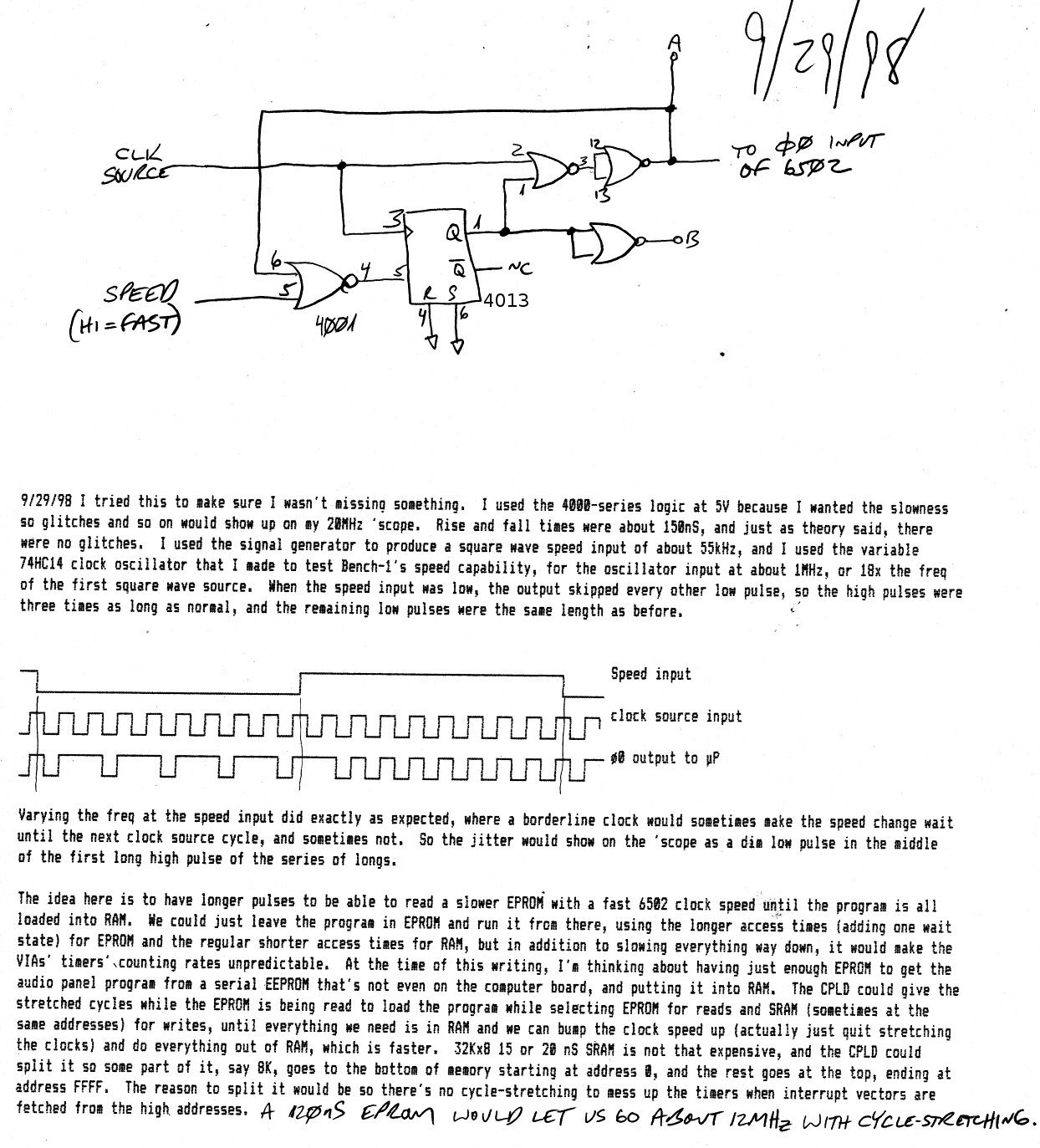
6502.org Forum  Projects  Code  Documents  Tools  Forum
It is currently Sat May 18, 2024 3:05 am

All times are UTC


Post new topic Reply to topic  [ 297 posts ]  Go to page Previous  1 ... 15, 16, 17, 18, 19, 20  Next
Author Message
 Post subject:
PostPosted: Thu Sep 23, 2010 2:05 am 
Offline

Joined: Sat Jan 04, 2003 10:03 pm
Posts: 1706
OK, so I sketched something out really quick on the whiteboard, took phone-cam pictures of it, doctored it up in Gimp, and below should be somewhat legible. :)

Code:
Broken external image
http://www.falvotech.com/tmp/whiteboard-1.jpg

I don't know how many cycles you need to wait, so I picked four cycles arbitrarily. In this case, we want to hold RDY low for three of those four cycles. As long as RDY is low, the 65C02 or 65C816 will attempt to retry the transaction the following cycle.

HISTORICAL NOTE: This will not work with NMOS 6502s. RDY is sampled during phase 1 on these CPUs, which is one of the reasons it was rarely used (it required fast address decoders). CMOS versions are required for this to work.

Code:
Broken external image
http://www.falvotech.com/tmp/whiteboard-2.jpg

This circuit has not been built by me, but it should(tm) "just work."

The circuit is a Johnson ring counter used to keep track of which cycle of the transaction it's in. We use a Johnson counter because it allows us to effortlessly detect back-to-back accesses to the same (slow) address space. Using a different counter would result in a slow first access, but then all subsequent burst accesses would run at bus rate, which isn't what you want.

SLOW is a signal derived from address decoding. It qualifies Phase-2 -- we don't want this circuit running when we're not accessing the slow resource. For as long as SLOW remains asserted and we have a valid clock, the counter will count. The inverter and OR gate ensure RDY remains pegged high when we're not accessing the slow device as well. That way, we don't lock up the bus.

Notice, though, that the XOR gate is used to derive the RDY signal. It's high if, and only if, we reach the end of the long cycle.

INTERESTING NOTE: The above circuit is actually a 68000 DTACK# generator, suitably modified to account for the 6502/65816's inability to distinguish one valid bus cycle from another.

Code:
Broken external image
http://www.falvotech.com/tmp/whiteboard-3.jpg

This picture shows the timing diagram of what happens inside the circuit. Notice that RDY represents the XOR of Qa and Qd#. You can see on the far right how it works with a burst access, assuming SLOW remains asserted in the subsequent cycle.

Let me know if this helps explain the idea better.


Top
 Profile  
Reply with quote  
 Post subject:
PostPosted: Thu Sep 23, 2010 6:38 am 
Offline

Joined: Tue Jul 05, 2005 7:08 pm
Posts: 994
Location: near Heidelberg, Germany
kc5tja wrote:
OK, so I sketched something out really quick on the whiteboard, took phone-cam pictures of it, doctored it up in Gimp, and below should be somewhat legible. :)


The ideal cycle timing looks ok to me.

I've done similar RDY-based CPU slow down to access a slow Philipps I2C controller chip: http://www.6502.org/users/andre/icaphw/rdy.html
When I have more time I need to compare your circuit to mine...

Recently I have used RDY to slow down a 65816 to accommodate for the slow system bus clock, either in a CPLD (Xilinx) http://www.6502.org/users/andre/csa/cpu816v2/index.html or with discrete logic in the predecessor of the CPLD-based board: http://www.6502.org/users/andre/csa/cpu816/index.html

I should probably update that article...

For my 65816-based CPU replacement board I use clock stretching though - it requires to synchronize the CPU to two asynchronous clocks, which does not work with RDY

André


Top
 Profile  
Reply with quote  
 Post subject:
PostPosted: Thu Sep 23, 2010 6:53 am 
Offline

Joined: Sat Jan 04, 2003 10:03 pm
Posts: 1706
I'm not convinced that RDY cannot be used to work with multiple clock domains.

If you modify the above circuit to use four edge-triggered D flip flops clocked such that FFA is clocked by phase2-A, FFB by phase1-B, FFC by phase2-B, and FFD by phase2-A, you will generate sufficient wait-states to pass traffic between clock domains A and B. Furthermore, A need not be faster than B; they could well be equal, or B could be faster than A.

Whether or not this approach is a preferred approach seems subjective to me; I definitely prefer RDY since it's more "correct." I don't like munging with the clock signal if I can avoid it.


Top
 Profile  
Reply with quote  
 Post subject:
PostPosted: Thu Sep 23, 2010 6:18 pm 
Offline

Joined: Tue Jul 05, 2005 7:08 pm
Posts: 994
Location: near Heidelberg, Germany
kc5tja wrote:
I'm not convinced that RDY cannot be used to work with multiple clock domains.


You're right that you can pass data between clock domains using RDY but most likely you'd have to store the data between "clock-domain-1-phi2-going-low" and "clock-domain-2-phi2-going-low" - and vice versa.

Using clock stretching I did not need a register to save the data between the domains, and was able to connect the two buses together.

André


Top
 Profile  
Reply with quote  
 Post subject: RDY Generation
PostPosted: Thu Sep 23, 2010 8:09 pm 
Offline
User avatar

Joined: Thu May 28, 2009 9:46 pm
Posts: 8190
Location: Midwestern USA
kc5tja wrote:
HISTORICAL NOTE: This will not work with NMOS 6502s. RDY is sampled during phase 1 on these CPUs, which is one of the reasons it was rarely used (it required fast address decoders). CMOS versions are required for this to work.

Also, NMOS MPUs don't stop on write cycles when RDY is asserted. Good luck trying to wait-state a write to slow hardware.

Quote:
Image
This circuit has not been built by me, but it should(tm) "just work."

The logic looks okay to me. However, there appears to be a booby trap in the circuit. From the WDC data sheet:

2.24 Ready (RDY)
The Ready is a bi-directional signal. When it is an output it indicates that a Wait for Interrupt instruction has been executed halting operation of the microprocessor. A low input logic level will halt the microprocessor in its current state. Returning RDY to the active high state releases the microprocessor to continue processing following the next PHI2 negative transition. The RDY signal is internally pulled low following the execution of a Wait for Interrupt instruction, and then returned to the high state when a RESB, ABORTB, NMIB, or IRQB external interrupt is active. This feature may be used to reduce interrupt latency...The RDY pin has an active pull-up and when outputting a low level, the pull-up is turned off to reduce power. The RDY pin can be wired ORed.


It would seem executing WAI with this circuit would result in the MPU trying to sink the output of that last OR gate when it's high (no wait-state wanted).

_________________
x86?  We ain't got no x86.  We don't NEED no stinking x86!


Top
 Profile  
Reply with quote  
 Post subject: 65xx wait-States
PostPosted: Thu Sep 23, 2010 8:27 pm 
Offline
User avatar

Joined: Thu May 28, 2009 9:46 pm
Posts: 8190
Location: Midwestern USA
ElEctric_EyE wrote:
kc5tja, thank you for responding. It was brought up by Dr. Jefyll a few posts ago, but...

I am unfamiliar with slowing the 6502 down this way. From what little I understand, I could force a hardware RDY state by WAI command, or send a hardware signal straight to the RDY pin?

I'm unsure how to go about this.

With CMOS parts, sinking RDY from an external source will cause the MPU to halt and maintain the address and data bus states. This will give slow hardware time to react to what was placed on the address bus. When RDY is allowed to return to the high state the MPU will resume exactly where it was stopped.

I should note that the WDC timing diagrams imply that RDY should not be asserted while Ø2 is low. In the case where the bank address feature of the W65C816S is being used, RDY probably should not be asserted until Ø2 high, as the A16-A23 address placed on D0-D7 is valid only during Ø2 low. Timing analysis suggests that if you assert RDY during Ø2 low, the bank address latch won't be latched if using the WDC recommended circuit.

Now, if a WAI instruction is executed, the MPU will halt until a hardware interrupt is received. During the time the MPU is halted by WAI it will pull RDY low. Hence RDY is actually a an input and an output.

RDY is internally pulled up to Vcc, but should be given an external pullup (2.2K to 3.3K is good) to assure it cleanly transitions between states. DO NOT tie RDY directly to Vcc, as doing so will cause MPU damage if a WAI is executed.

On my POC design, I used a 3.3K pullup because I had some SIPs of that value in my CC (crap collection, as so delicately named by my dear wife).

_________________
x86?  We ain't got no x86.  We don't NEED no stinking x86!


Top
 Profile  
Reply with quote  
 Post subject: Re: RDY Generation
PostPosted: Thu Sep 23, 2010 8:52 pm 
Offline

Joined: Sat Jan 04, 2003 10:03 pm
Posts: 1706
BigDumbDinosaur wrote:
It would seem executing WAI with this circuit would result in the MPU trying to sink the output of that last OR gate when it's high (no wait-state wanted).


The circuit is fine.

I mentioned earlier (in another thread? I can't remember) that you're expected to drive RDY through a (IIRC, 470 ohm) resistor at the CPU pin. I didn't show the resistor here because it's needless detail, and if you have multiple sources of RDY generation, it doesn't make any sense to put it here anyway.

:)


Top
 Profile  
Reply with quote  
 Post subject:
PostPosted: Thu Sep 23, 2010 8:56 pm 
Offline
User avatar

Joined: Fri Aug 30, 2002 1:09 am
Posts: 8438
Location: Southern California
Here's a scan of something I did 12 years ago for a project that got cancelled before I finished. I had emailed it to Electric_Eye but decided to post it. It does not use RDY.

Image


Top
 Profile  
Reply with quote  
 Post subject:
PostPosted: Fri Sep 24, 2010 1:57 am 
Offline

Joined: Mon Mar 02, 2009 7:27 pm
Posts: 3258
Location: NC, USA
I'll be honest guys, I don't like slowing down a cpu "artificially" with wait states. My view may change in the future when I learn more, but right now I'd prefer to set a "speed" bit than wait states...

But after looking at Garth's last post, I am questioning a "cycle stretcher" vs. a "synchronizer". A synchronizer is what I posted yesterday. It takes 2 asynchronous frequencies and based on a select signal smoothly transitions without any spikes or runt signals between either frequency.

Is this the same as a cycle stretcher?
Quoting from Garth's last post where it's handwritten, "a 120nS EPROM would let us go about 12MHz...". A 120nS EPROM, assuming your address decoding logic is 0nS, could be addressed maximally at no more than 8.333MHz...

_________________
65Org16:https://github.com/ElEctric-EyE/verilog-6502


Top
 Profile  
Reply with quote  
 Post subject:
PostPosted: Fri Sep 24, 2010 2:00 am 
Offline

Joined: Sat Jan 04, 2003 10:03 pm
Posts: 1706
ElEctric_EyE wrote:
I'll be honest guys, I don't like slowing down a cpu "artificially" with wait states. My view may change in the future when I learn more, but right now I'd prefer to set a "speed" bit than wait states...


A speed bit is no more artificial than wait-states. I'm curious to learn why wait states isn't something you're comfortable with.


Top
 Profile  
Reply with quote  
 Post subject:
PostPosted: Fri Sep 24, 2010 2:37 am 
Offline

Joined: Mon Mar 02, 2009 7:27 pm
Posts: 3258
Location: NC, USA
I think in terms of speed only to keep it simple. If I know my EEPROM has an access time of 200nS, then max speed without any artificial hardware tricks is close to 5MHz. Right now, I push no more than 1/2 of that. Instead of figuring delay cycles, it's easier for me to think in MHz. So I set the speed bit for 2.5MHz when I need to read from the 200nS EEPROM. Right after the copy program is done reading from the EEPROM, I throttle the speed back to as fast as the WDC65C02 will go, which is nowhere near the speed of a 2M 10nS SRAM...

Hence my last question, how does one run a 120nS EPROM at 12MHz without using the RDY signal?

_________________
65Org16:https://github.com/ElEctric-EyE/verilog-6502


Last edited by ElEctric_EyE on Fri Sep 24, 2010 4:19 am, edited 1 time in total.

Top
 Profile  
Reply with quote  
 Post subject:
PostPosted: Fri Sep 24, 2010 3:41 am 
Offline
User avatar

Joined: Fri Aug 30, 2002 1:09 am
Posts: 8438
Location: Southern California
Quote:
Hence my last question, how does one run a 120nS EPROM at 12MHz without using the RDY signal?

12MHz is the frequency of the oscillator. With the speed input to my circuit low, you actually get 6MHz, but instead of being symmetrical, it will be high 75% of the time and low only 25%, giving you three times as long a phase-2-high time to work with as you get at 12MHz with a symmetrical square wave.

In your application, you can do with a single oscillator (fewer parts), and start with the speed input to the circuit low until you're done loading the RAM from ROM, then set that input high (which you can do at any time without producing a glitch), and leave it high full-time until the next boot-up. The job of giving the ROM more time to spit out its data is then only on this circuit and not on the processor.

I used 4000-series logic only for the low speed, to make sure I would be able to see any glitches or runt pulses on my inexpensive oscillosclope. I would never use 4000-series stuff on a computer board. The idea was that once the idea is proven, I would move it to at least 74HC if not faster. Actually for that project, I was going to put this and a bunch of other logic in a Cypress CPLD. 4000-series logic is very slow at 12V and ultrasuperslow at 5V. I only use it for interfacing to 12V analog stuff where speed is not an issue.


Top
 Profile  
Reply with quote  
 Post subject:
PostPosted: Fri Sep 24, 2010 4:29 am 
Offline

Joined: Sat Jan 04, 2003 10:03 pm
Posts: 1706
Interesting; I can't think that way myself. I think of time as an agglutinable resource, where I can snap together units of time to make longer units of time.

In this case, the basic unit of time is the CPU cycle, which I intend to be as small as RAM would permit. If ROM or I/O needs longer to respond, then using RDY to insert wait states would be an acceptable sacrifice to me. It also means I don't have to manually flip bits, which lessens my chance for error.

RDY is particularly useful for I/O with variable latency, though.

Oh, I should also point out that clock stretching/switching is valid; I'm certainly not bashing the technique. I just prefer not to use it. The Apple IIgs worked great, for example, switching automatically between 2.8MHz and 1.0MHz via clock switching, so prior art definitely exists to vindicate the technique.


Top
 Profile  
Reply with quote  
 Post subject:
PostPosted: Fri Sep 24, 2010 8:43 pm 
Offline

Joined: Tue Jul 05, 2005 7:08 pm
Posts: 994
Location: near Heidelberg, Germany
Here's one reason to go with clock stretching, i.e. extending Phi2 high when accessing slower devices.

If the device's select lines are qualified with phi2, it is much easier to work with a stretched phi2, than to separately extend the select signals when RDY is asserted

André


Top
 Profile  
Reply with quote  
 Post subject:
PostPosted: Fri Sep 24, 2010 8:49 pm 
Offline

Joined: Sat Jan 04, 2003 10:03 pm
Posts: 1706
But, it's the same logic. The select line is driven by the address decoder output. You, in fact, must add logic to extend the clock (in a phase-locked manner to avoid glitches) separately. The amount of logic is exactly the same.


Top
 Profile  
Reply with quote  
Display posts from previous:  Sort by  
Post new topic Reply to topic  [ 297 posts ]  Go to page Previous  1 ... 15, 16, 17, 18, 19, 20  Next

All times are UTC


Who is online

Users browsing this forum: No registered users and 6 guests


You cannot post new topics in this forum
You cannot reply to topics in this forum
You cannot edit your posts in this forum
You cannot delete your posts in this forum
You cannot post attachments in this forum

Search for:
Jump to: