6502.org Forum  Projects  Code  Documents  Tools  Forum
It is currently Sun Apr 28, 2024 8:43 am

All times are UTC


Post new topic Reply to topic  [ 564 posts ]  Go to page Previous  1 ... 7, 8, 9, 10, 11, 12, 13 ... 38  Next
Author Message
 Post subject:
PostPosted: Fri Aug 13, 2010 2:23 pm 
Offline
User avatar

Joined: Fri Aug 30, 2002 9:02 pm
Posts: 1681
Location: Sacramento, CA
My SBC-2 and SBC-3 both have a disassembler - 65C02 opcodes on the SBC-2 and 65816 on the SBC-3.

In addition, the SBC-2 has a mini-assembler, very similar to the Apple ][ mini-assembler, that supports the 65C02 opcodes. Mini means it will assemble opcodes and hexidecimal values - no labels or variables are supported. Branch instructions are entered using the target address, so it will compute the proper offset.

If desired, an assembly source could be sent via the RS-232 port and the assembler will assemble it on the fly into RAM. It does not use handshaking so a plain text transfer is done with inter-character and inter-line delays in the terminal emulator.

Source code would look something like this:

Code:
1000: LDA #FF
 STA 00
 LDA 01
 BNE 1010
 RTS
1010: DEC 00
 RTS


Crude, but effective for simple routines or quick test code.

Sources are on my website - look in the Downloads tab under sbc2os.zip and sbc3.zip

It would not be too hard to port to another platform.

If you want to see the assembler/disassembler code working, download my 65C02 Simulator. It has the sbc2os running on it.

Daryl


Top
 Profile  
Reply with quote  
 Post subject: POC V1.0
PostPosted: Fri Aug 13, 2010 5:08 pm 
Offline
User avatar

Joined: Thu May 28, 2009 9:46 pm
Posts: 8147
Location: Midwestern USA
8BIT wrote:
My SBC-2 and SBC-3 both have a disassembler - 65C02 opcodes on the SBC-2 and 65816 on the SBC-3.

In addition, the SBC-2 has a mini-assembler, very similar to the Apple ][ mini-assembler, that supports the 65C02 opcodes. Mini means it will assemble opcodes and hexidecimal values - no labels or variables are supported. Branch instructions are entered using the target address, so it will compute the proper offset.

Same with the assembler in my POC's BIOS ROM. It will compute both 8 and 16 bit branch offsets, plus accept 16 bit immediate mode operands where allowed (all immediate mode instructions except REP and SEP).

Technically speaking, an assembler is not required to understand labels or variables. So, calling your assembler a mini-assembler is being mean and disrespectful to it. :) It does the job of translating LDA #65 into A9 41 and poking that byte sequence into RAM at an address of your choosing, which means it is a real assembler. Anything it can do over and above that is frosting on the cake.

_________________
x86?  We ain't got no x86.  We don't NEED no stinking x86!


Top
 Profile  
Reply with quote  
 Post subject:
PostPosted: Sat Aug 14, 2010 12:59 am 
Offline
User avatar

Joined: Fri Aug 30, 2002 9:02 pm
Posts: 1681
Location: Sacramento, CA
That may be true, but since Apple called it a mini-assembler, and mine is spun from it, that is what I call it too. It seems to be ok with that label. :lol:


Top
 Profile  
Reply with quote  
 Post subject: POC V1.0
PostPosted: Sat Aug 14, 2010 1:31 am 
Offline
User avatar

Joined: Thu May 28, 2009 9:46 pm
Posts: 8147
Location: Midwestern USA
8BIT wrote:
That may be true, but since Apple called it a mini-assembler, and mine is spun from it, that is what I call it too. It seems to be ok with that label. :lol:

One feature I did add to mine is the ability to accept numeric parameters in any of four bases, so:

Code:
LDA #$0a
LDA #+10
LDA #@12           ;octal
LDA #%00001010

all mean the same to the assembler.

In the absence of the radix symbol the assembler assumes hex, so LDA #a is the same as LDA #$0A.

_________________
x86?  We ain't got no x86.  We don't NEED no stinking x86!


Top
 Profile  
Reply with quote  
 Post subject:
PostPosted: Sat Aug 14, 2010 1:36 am 
Offline
User avatar

Joined: Fri Aug 30, 2002 1:09 am
Posts: 8428
Location: Southern California
I started out in 1982 in a microprocessor class doing hand-assembly. You quickly memorize all your commonly used op codes; but the big problem was adjusting JMP and JSR addresses and branch distances if you had to insert anything, since that pushed the following code farther out. Deleted instructions could be replaced with NOPs, and variables tend to come before the code so their addresses stay put a little better. I got in the habit of sprinkling NOPs in, especially after RTS and JMP instructions, so an insertion did not require moving and adjusting so much.

From that experience, I would say a minimal assembler's first value would be in having a way to calculate the jump and branch addresses, based on labels or placeholders of some sort, and of course the automatic address counting.

I wrote my initial programs by hand for my first computer a few years later, and, since I didn't have a computer of any kind at all running yet, I had no assembler. My EPROM programmer was hand-operated too, requiring that you enter the address and data with switches, then push the button for the 50ms programming pulse, then go to the next byte. It was very slow, and required extreme care to avoid mistakes. I did get this computer going this way, although it never did anything useful. My programs were written on paper, like flowcharts with op codes and operands in the boxes, and when ready, I would transfer the hex numbers to sheets with 16x16 grids, each sheet pertaining to a page of 6502 memory.

_________________
http://WilsonMinesCo.com/ lots of 6502 resources
The "second front page" is http://wilsonminesco.com/links.html .
What's an additional VIA among friends, anyhow?


Top
 Profile  
Reply with quote  
 Post subject:
PostPosted: Sat Aug 14, 2010 5:55 pm 
Offline
User avatar

Joined: Thu May 28, 2009 9:46 pm
Posts: 8147
Location: Midwestern USA
GARTHWILSON wrote:
I started out in 1982 in a microprocessor class doing hand-assembly.

Gotcha beat on that one. :) I used a patch board way back in 1970 to code a post office mail ZMT (ZIP mail translator). Normally we used a Tele-Type to load a program into core but that day the TTY went on the fritz and we had to wait for parts to fix it. So I rigged up a simply patch board using some 1/4 inch phone plugs and jacks, along with two toggle switches, to simulate the bitwise output provided to the ZMT by our customized TTY. Plug or unplug the "bits" and flip the first switch to set the core address, and then flip the second switch to write the bit pattern to core. Move plugs around to change the address and next bit pattern, and repeat. Talk about slow! It took several hours to load a 256 byte program. The only way to tell if it was right was to try sorting some mail and see where it ended up.

Quote:
My EPROM programmer was hand-operated too...

By the time I got around to burning EPROMs, I had concocted a burner that ran off the user port of a C-64 and could use a hybrid BASIC/machine language program to do the dirty work. It seemed so luxurious back then. :lol:

_________________
x86?  We ain't got no x86.  We don't NEED no stinking x86!


Top
 Profile  
Reply with quote  
 Post subject: POC V1.0
PostPosted: Thu Sep 16, 2010 6:32 am 
Offline
User avatar

Joined: Thu May 28, 2009 9:46 pm
Posts: 8147
Location: Midwestern USA
"Real" work has been getting in the way as of late, but I've still found some time to fool around with POC 1.0.

I've completely recoded the BIOS ROM so the MPU switches to and stays in native mode following reset. Since the MPU is running in native mode, I can take advantage of the 16 bit stack pointer, as well as other enhanced features. Top of RAM on this unit is at $CFFF, so that is the top of the stack. Code and data can build up from $0100 until a stack collision occurs (would take a lot of pushes to accomplish that). For now, page zero is staying at $00 in RAM.

The built-in machine language monitor also reflects the switch to native mode. 16 bit code has been used where it is beneficial and it is apparent that in some operations (memory transfer and fill), a significant performance improvement was gained. In fact, the memory transfer function uses the MVN and MVP operations to do the dirty work.

Right now, the monitor supports the following operations:
    A assemble code
    C compare memory areas
    D disassemble code
    G run code (stops on a BRK)
    H search memory for pattern, accepts byte values or ASCII strings
    J run code as a subroutine (stops on an RTS)
    L load Motorola S-record code through the 2nd EIA-232 port
    M dump memory
    R dump MPU registers
    T transfer (copy) memory
    Z clear the screen
    > change memory
    ; change registers
The L(oad) function allows me to assemble code into S-record format on my UNIX development system and then copy it to the POC through a high-speed EIA-232 link (115.2 Kbps). The ROM translates the S-records to binary on the fly, and can do a relocating load. This feature will come in handy when I start working on the SCSI interface. :)

Here are a few screen shots of the monitor in use:

POST screen after falling into the monitor due to no SCSI hardware being present.

Assembling some 16 and 24 bit instructions.

Assembling a SEP instruction and taking advantage of built-in radix conversion.

Executing the program I just assembled. The register dump shows a bit more than what you might see with a 65C02. The XBA instruction comes in handy for displaying 16 bit values in human-readable format.

Sorry for some of the blurriness in the pics, but I'm back on chemo in my never-ending battle with Pac-Man. The side-effects make holding things steady a bit of a challenge at times.

_________________
x86?  We ain't got no x86.  We don't NEED no stinking x86!


Top
 Profile  
Reply with quote  
 Post subject: POC Version 2
PostPosted: Thu Oct 14, 2010 2:54 am 
Offline
User avatar

Joined: Thu May 28, 2009 9:46 pm
Posts: 8147
Location: Midwestern USA
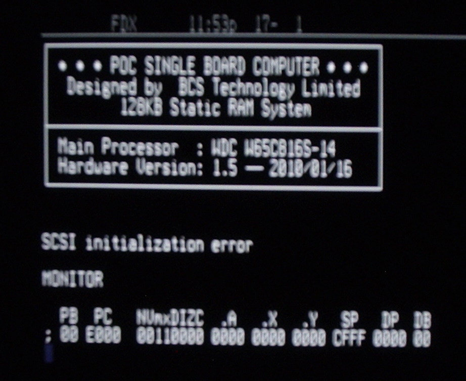
Now that version 1 of the POC unit appears to be working well, I'm ready to extend the design to the next level, which is to work out some means of providing mass storage facilities. For me, that means SCSI hardware. Accordingly, I have acquired some 53C94 SCSI ASICs, along with a 63 page data sheet.

The 53C94 is new to me, but is conceptually similar to the older 53C90A, with which I am familiar. Both ASICs work with the "narrow" SCSI bus, but the 53C94 has a variant that can support an HVD bus, which can operate over a 75 foot (!) cable. The other difference between the two is the 53C94 supports both SCSI-1 and SCSI-2 commands, whereas the 53C90A only supports SCSI-1 (the original 1986 ANSI standard). As any SCSI device manufactured since the mid-1990s will understand SCSI-2, I will use that as my programming model. Also, as it so happens, I have some 
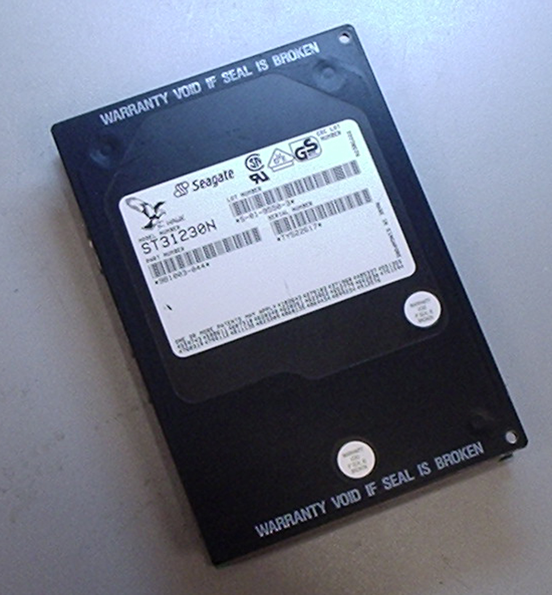
narrow SCSI-2 hard drives in my junk pile with which to experiment (the pictured drive came from a server I had in operation 15 years ago).

The 53C94 was designed to automate the SCSI bus protocol so the host machine wouldn't have to engage in all the required signaling and bit twiddling. Initial communication with a SCSI target is made by loading a command descriptor block into the chip's FIFO, telling it the target SCSI ID and then telling the chip to start the arbitration and selection sequence. Once selection has been completed, the chip will generate a SCSI phase change interrupt and two way communication can commence. If the target device fails to respond, selection will eventually time out and the 53C94 will again generate an interrupt.

Hardware-wise, the 53C94 was targeted to the Motorola 68K MPU (as was the 53C90A) and was meant to communicate with the host bus via 8 or 16 bit DMA. The controller can be also be configured to operate in PIO mode, which is how I plan to use it (no 65xx compatible DMA controller handy). If it were possible to run it via DMA, throughput onto the bus could reach upwards of 20 MB/sec. <Sigh>

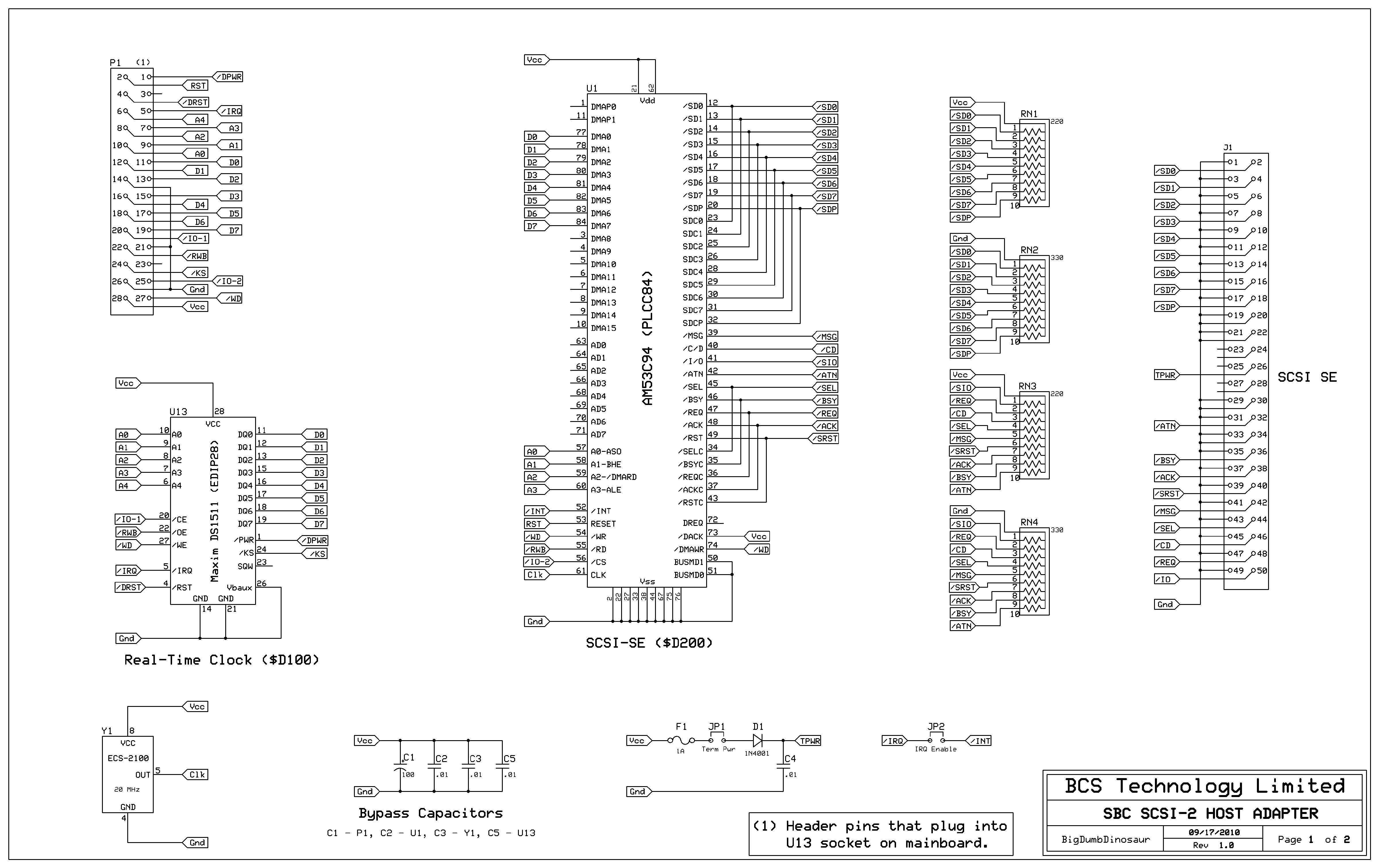
The SCSI side of the chip is straightforward to implement. The 53C94 is able to directly drive the SCSI bus without extra hardware, other than bus termination resistors (take a look-see at this schematic I concocted). As is characteristic of 8 bit SCSI implementations, 50 pin connectors and associated ribbon cable are used to connect all devices to the host.

Adapting the 53C94 to the '816 isn't too difficult. Chip selects work the same as on the 2692A DUART that I am using for serial I/O (the 2692 was also targeted to the 68K), so no additional glue logic will be required on the MPU side. Ironically, when run in PIO mode, the chip's data path is through the lower eight bits of the DMA port and the "data bus" on the chip is not used at all. It seems kind of odd at first but makes more sense once one is familiar with the part.

The 53C94 requires a clock input between 10 MHz and 25 MHz. This clock is used for internal timing purposes and to correctly sequence the SCSI bus. While I could derive that clock from Ø2, it will be more convenient to provide a separate oscillator for the purpose. This is because the chip has to be told what frequency range to expect, which if from Ø2, means I'd have to recode the firmware if I were to change the clock. As with the 2692, a separate clock means operation of the 53C94 is asynchronous to the 65C816 bus, and the same timing gotchas that gave me trouble with the 2692 are potentially present.

The actual circuit will be part of a new-design mainboard. I was toying with the idea of hand-building this thing and adapting it to the current POC unit, but don't feel like struggling with that 84 pin PLCC socket and all those pins on the SCSI port.

The real work will be in crafting a suitable driver. The SCSI bus operates in phases and the 53C94 will generate an IRQ each time the bus changes phase, an operating mode that suggests that the driver should be a mixture of foreground and IRQ code. The IRQ part would act as a dispatcher to select the part of the foreground code that is appropriate for the current bus phase. I'm envisioning where the dispatcher would change the return address on the MPU stack by using the phase bits (which can be read out of a particular 53C94 register) as an index into a dispatch table. Thanks to the 65C816's improved stack features, this will be less a job to code than an equivalent running on a 65C02. It isn't going to be a piece of cake, though.

When operated in synchronous mode, SCSI-2 can achieve a 10 MB/sec transfer rate across the bus (the data sheet incorrectly says 5 MB/sec). In reality, this can't happen using PIO, as none of the 65C816 load/store instructions can execute quickly enough to sustain that rate (hence the value of DMA). The model that I've worked out so far suggests about 750 KB/sec average throughput with the MPU running at 20 MHz. The select and setup times on the 'C94 in PIO mode will require at least one wait state to run at that high a clock rate. 750 KB/sec isn't too bad, though. At that rate, an entire 64K frame could be loaded in less than 100 milliseconds. In practice, much smaller amounts of data are handled per bus transaction, so the performance should be just fine.

_________________
x86?  We ain't got no x86.  We don't NEED no stinking x86!


Last edited by BigDumbDinosaur on Tue Feb 04, 2020 7:17 pm, edited 1 time in total.

Top
 Profile  
Reply with quote  
 Post subject:
PostPosted: Fri Oct 15, 2010 1:08 am 
Offline

Joined: Mon Mar 02, 2009 7:27 pm
Posts: 3258
Location: NC, USA
SCSI for me has always meant higher transfer rates along with HDD RPM spin rates @10,000+. More $$$

Sounds like you're maybe aiming for a day when you do actually have a DMA controller?. Else, a regular ole' EIDE HDD would be ok with the multiple PIO modes right?

I'm looking into a controller in a 100-pin QFP package for similar purposes. The IC you've chosen though has a patented "GLITCH eater" circuit, that apparently helps in the transmission of data and compensates for voltage spikes and reflections in the ribbon cable. Looks interesting...

Where can one find the IC you've chosen? How much is it?

_________________
65Org16:https://github.com/ElEctric-EyE/verilog-6502


Top
 Profile  
Reply with quote  
 Post subject: POC Version 2
PostPosted: Fri Oct 15, 2010 2:29 am 
Offline
User avatar

Joined: Thu May 28, 2009 9:46 pm
Posts: 8147
Location: Midwestern USA
ElEctric_EyE wrote:
SCSI for me has always meant higher transfer rates along with HDD RPM spin rates @10,000+. More $$$

As with almost everything else in computers, you get what you pay for. SCSI is a very robust system and supports a lot of different kind of hardware. I have a lot of experience with SCSI, going back to the mid-1980s.

Quote:
Sounds like you're maybe aiming for a day when you do actually have a DMA controller? Else, a regular ole' EIDE HDD would be ok with the multiple PIO modes right?

EIDE is a bit of a pain to implement. SCSI is standardized around a device-agnostic command and bus system. EIDE disks don't support the intelligence of SCSI and for that reason, I'm not interested in them. Also, where would you get an intelligent EIDE controller comparable to the 53C94 that you could interface to a 65xx bus?

As for a DMA controller, I've got this vague idea that one could probably be implemented in a CPLD or FPGA. At this point in time, however, I've not given it any thought, nor do I know enough about CPLDs and FPGAs to begin to design one.

Quote:
I'm looking into a controller in a 100-pin QFP package for similar purposes. The IC you've chosen though has a patented "GLITCH eater" circuit, that apparently helps in the transmission of data and compensates for voltage spikes and reflections in the ribbon cable. Looks interesting...

The glitch-eater prevents false phase changes due to switching spikes on the /ACK and /REQ control lines, which are vulnerable to this sort of thing. Without it, ramping up the bus speed would have been difficult on anything except really short cables.

Quote:
Where can one find the IC you've chosen? How much is it?

I got them from Quest Components. Look for part number AM53C94JC (J = PLCC84). I paid 10 bucks each.

_________________
x86?  We ain't got no x86.  We don't NEED no stinking x86!


Top
 Profile  
Reply with quote  
 Post subject: Re: POC Version 2
PostPosted: Fri Oct 15, 2010 6:22 pm 
Offline

Joined: Thu Jul 26, 2007 4:46 pm
Posts: 105
BigDumbDinosaur wrote:
Quote:
Sounds like you're maybe aiming for a day when you do actually have a DMA controller? Else, a regular ole' EIDE HDD would be ok with the multiple PIO modes right?

EIDE is a bit of a pain to implement. SCSI is standardized around a device-agnostic command and bus system. EIDE disks don't support the intelligence of SCSI and for that reason, I'm not interested in them. Also, where would you get an intelligent EIDE controller comparable to the 53C94 that you could interface to a 65xx bus?


You don't need a smart controller for parallel ATA; its basically a subset of 16-bit ISA run out over a ribbon cable. The only real complexity is the bufers in order to translate between the 8-bit and 16-bit busses. It would run comfortably (though slowly) hung off some GPIO pins.

Sure the disks don't have the intelligence of SCSI disks; yet I fail to see why, in this application, it would be useful...

Quote:
As for a DMA controller, I've got this vague idea that one could probably be implemented in a CPLD or FPGA. At this point in time, however, I've not given it any thought, nor do I know enough about CPLDs and FPGAs to begin to design one.


One would be pretty trivial in an FPGA. The fact that it uses a separate "DMA" bus is quite odd though; most devices of this vintage are designed for flyby DMA (i.e. the DMA controller generates addresses, but the device directly drives the data bus). Obviously, more modern devices have gone to full bus mastering

I would personally have gone for something like an SD card though; for your applications, more than sufficient, much cheaper, and much simpler to drive. They'll easily keep up with what the 65c816 can do also.


Top
 Profile  
Reply with quote  
 Post subject: Re: POC Version 2
PostPosted: Fri Oct 15, 2010 8:04 pm 
Offline
User avatar

Joined: Thu May 28, 2009 9:46 pm
Posts: 8147
Location: Midwestern USA
OwenS wrote:
You don't need a smart controller for parallel ATA; its basically a subset of 16-bit ISA run out over a ribbon cable. The only real complexity is the bufers in order to translate between the 8-bit and 16-bit busses. It would run comfortably (though slowly) hung off some GPIO pins.

It's the "though slowly" part that I don't want.

Quote:
Sure the disks don't have the intelligence of SCSI disks; yet I fail to see why, in this application, it would be useful...

To which application are you referring?

That the work required to communicate with the disk (CD-ROM or anything else that can be attached to a SCSI bus) is off-loaded to hardware means the '816 has to do less to achieve good I/O throughput. With IDE, I'd be faced with bit-banging it (as well as double-buffer to deal with the 16 bit bus to 8 bit bus transition), and disk I/O would suck.

Quote:
Quote:
As for a DMA controller, I've got this vague idea that one could probably be implemented in a CPLD or FPGA.

One would be pretty trivial in an FPGA. The fact that it uses a separate "DMA" bus is quite odd though; most devices of this vintage are designed for flyby DMA (i.e. the DMA controller generates addresses, but the device directly drives the data bus). Obviously, more modern devices have gone to full bus mastering.

The 53C94's dual bus design makes sense when you consider that SCSI-2 introduced queued commands. With the DMA bus available as a separate and direct I/O path, it is possible with the right hardware to issue a new command to the 'C94 while it is processing the I/O from the previous one. The result would be a dramatic improvement in back-to-back command performance.

Quote:
I would personally have gone for something like an SD card though; for your applications, more than sufficient, much cheaper, and much simpler to drive. They'll easily keep up with what the 65c816 can do also.

Again, what applications? Are you saying I shouldn't do SCSI at all? It sounds as though you are discouraging experimentation. :)

I don't know about the cost of an SD card, so I can't make a comparison. Consider that I have SCSI drives around here that were removed from functioning systems, as well as suitable cables to connect them. So there's no money involved with them. Aside from the ASICs, my only additional cost will be the parts I don't have, which represent very little cost.

_________________
x86?  We ain't got no x86.  We don't NEED no stinking x86!


Top
 Profile  
Reply with quote  
 Post subject:
PostPosted: Fri Oct 15, 2010 8:59 pm 
Offline

Joined: Tue Jul 05, 2005 7:08 pm
Posts: 990
Location: near Heidelberg, Germany
ElEctric_EyE wrote:
SCSI for me has always meant higher transfer rates along with HDD RPM spin rates @10,000+. More $$$


Yes, SCSI has always had better a better interface design. It's even so simple I have built an async-mode SCSI board for my 6502 computer and use SCSI disks as storage.

It is so compatible that even a 4GB SCSI-II wide IBM harddisk works (with an adapter from wide to narrow SCSI) in SCSI-I async mode with my board!

Unfortunately modern hardware has switched to SASI/SATA, so a real controller is unavoidable it seems, or using USB or Ethernet-attached storage.

André


Top
 Profile  
Reply with quote  
 Post subject: Re: POC Version 2
PostPosted: Fri Oct 15, 2010 9:06 pm 
Offline

Joined: Tue Jul 05, 2005 7:08 pm
Posts: 990
Location: near Heidelberg, Germany
BigDumbDinosaur wrote:
I don't know about the cost of an SD card, so I can't make a comparison.


I think he means the SD flash memory cards.
http://en.wikipedia.org/wiki/Secure_Digital
Yes, they are easy to interface as well, at least the SD variety with their SPI mode interface

Wikipedia says: "All cards must support all three modes, [one bit, four bit, SPI mode] except for microSD where SPI is optional."

Even the new (higher speed and higher capacity) SDHC/SDXC should support that: "All SD cards (other than microSD) can, at least, be accessed freely using the well-documented SPI/MMC mode"

I've also done an SD card interface for my 6502 system :-)

André


Top
 Profile  
Reply with quote  
 Post subject:
PostPosted: Fri Oct 15, 2010 9:21 pm 
Offline
User avatar

Joined: Fri Aug 30, 2002 1:09 am
Posts: 8428
Location: Southern California
Quote:
I don't know about the cost of an SD card

SD cards are slightly bigger than the common postage stamp and 4GB will cost something like $20.

If you don't need SD in particular, you can get tiny, dense SPI flash memories to act as an internal hard disc for your own projects. I have a 4Mx8 SPI flash memory in an SO-8 working that takes about .08 sq. in. of board space, not much more than a T1-3/4 LED.

_________________
http://WilsonMinesCo.com/ lots of 6502 resources
The "second front page" is http://wilsonminesco.com/links.html .
What's an additional VIA among friends, anyhow?


Top
 Profile  
Reply with quote  
Display posts from previous:  Sort by  
Post new topic Reply to topic  [ 564 posts ]  Go to page Previous  1 ... 7, 8, 9, 10, 11, 12, 13 ... 38  Next

All times are UTC


Who is online

Users browsing this forum: No registered users and 20 guests


You cannot post new topics in this forum
You cannot reply to topics in this forum
You cannot edit your posts in this forum
You cannot delete your posts in this forum
You cannot post attachments in this forum

Search for:
Jump to: