I read website -- http://www.pagetable.com/?p=39. It tells how illegal instruction sets work. It explains decode ROM PLA and timing generation logic.
I want to know how instruction register and timing generation logic communicate to ROM PLA through 21 wires.
Do timing generation logic always have one bit in one 8-bit register? If T0 is set, then instruction register is decoded during first cycle. One bit in timing register is shifted left during second cycle through 8 clock cycles. After it is shifted left, timing register is empty and then 6502 ceases to function like HLT instruction.
Do you have information how to obtain binary image from decode ROM PLA?
Bryan
Decode ROM PLA Question

Hi Bryan
the latest development in reverse-engineering the 6502 is covered in this thread (project team is Greg James, Barry Silverman and Brian Silverman)
With the transistor-level simulation(*) from that project I was able to trace the PLA inputs while running various test programs. There are 6 inputs relating to the state of the machine, and 15 inputs from the IR which holds the instruction being executed.
Normally you'd expect 16 inputs from the IR - true and inverted versions of each bit - but one of them isn't needed so it isn't there.
The 6 timing inputs are (nearly) one-cold signals - one of them, or none of them, is zero (sometimes two are zero). Two of them are related to SYNC, and the other 4 come from a shift register. If there are no bugs in the machine, and it runs a legal 6502 program, and there isn't too much radiation, those state bits will never visit an illegal state. What happens in other circumstances, well, it's not part of the specification and you'd just have to discover what the logic happens to do.
One thing to look out for: in the first cycle of an instruction, SYNC is high and the instruction is read from RAM. This is normally referred to as T0. But in this cycle, the IR still holds the previous instruction, and the previous instruction may use this cycle to write a result back to a register. It might be better to think of this as the final cycle of the previous instruction.
See my last post in this thread for an example.
The idea is that visual6502.org will have explanations and examples of how different parts of the 6502 work. Right now, that's a placeholder page. I imagine a description of the machine sequencing (Timing Control) will be up there one day.
If you want the content of the PLA, right now the best source is Balazs' schematic - there's a link in the thread mentioned above. You'd need to do some image processing to get the binary information. If you wait a bit, the information might be more available from the visual6502 project.
If you want to know how it could be done, rather than precisely how it was done, check the various VHDL models for 6502. One of those, at least, uses a tabular approach.
Cheers
Ed
(*) will hopefully be released fairly soon
-
Bryan Parkoff
- Posts: 109
- Joined: 25 Dec 2007
Bryan Parkoff wrote:
>With the transistor-level simulation(*) from that project?
Did you write true 6502 simulator in software to behave like real hardware 6502 MPU?
Bryan
Did you write true 6502 simulator in software to behave like real hardware 6502 MPU?
Bryan
This simulator could simulate any chip which uses similar circuit techniques, if it's not too big and if you have an accurate transistor netlist.
In this case, the 6502 revD transistor netlist was recovered from photomicrographs of deprocessed 6502s, so yes, this simulation behaves like real hardware. They have run some Atari games on this simulation, and they are pixel-perfect. There could, in theory, still be bugs in the netlist, or situations which the simulator doesn't handle, but it's looking good. They have a suite of tests, which they used as regression tests while finishing the netlist and the simulator(s).
Bear in mind that this kind of low level simulation is not high performance - it runs at a few Hz. Not MHz, but Hz. To run at MHz, you need an emulator(*), which isn't going to work using the same physical bottom-up approach.
Cheers
Ed
(*) Edit: I should clarify that I'm still talking about software models here, but higher-level. I'm not talking about in-circuit-emulators, which is a hardware model operating at full speed.
Last edited by BigEd on Mon Sep 13, 2010 1:48 pm, edited 1 time in total.
-
Bryan Parkoff
- Posts: 109
- Joined: 25 Dec 2007
-
visual6502
- Posts: 3
- Joined: 13 Sep 2010
- Location: San Francisco, CA
- Contact:
Hi Bryan - Our website, www.visual6502.org , has just gone live with some basic info and our contact email. Enjoy, and more is on the way!
-Greg
-Greg
-
Bryan Parkoff
- Posts: 109
- Joined: 25 Dec 2007
I am just curious since I read all posts. We do not understand yet how six timing states work. IR and T states are wired to ROM PLA directly. I suspect that not all 15 inputs of IR are used or they are undefined.
If it is related to illegal instructions, my question is were 6502 simulator able to reproduce bugs?
ADC / SBC in decimal mode has bugs with invalid negative flag, overflow flg, and zero flag.
In my C++ code, I was able to reproduce bug and I claim that overflow flag and carry flag are valid, but negaitve flag and zero flag are invalid as bug. I did confirm to be 100% correct to reproduce bug because I created binary image when I simulated ADC / SBC in decimal mode.
Bryan
Hi Bryan
if you assemble your test case - which would be about 6 bytes I suppose - you can type the hex values into the simulator memory and step through the ADC or SBC.
if you like, I'll do it - just post your bytes! The answer we're expecting is that the visual6502 will give the same answer as a real 6502.
I'm not sure why you think some of the 15 IR signals don't make it to the PLA? I've seen them!
Cheers
Ed
Edit: typo!
Last edited by BigEd on Wed Sep 15, 2010 6:36 pm, edited 1 time in total.
-
ElEctric_EyE
- Posts: 3260
- Joined: 02 Mar 2009
- Location: OH, USA
The Javascript simulator tool on the site is very nice. You can zoom in, put your own code into zero page and see the stack and the whole interaction amongst pins. What makes it even more awesome is that it isn't just an emulator, this is from a single IC they have deconstructed.
The Javascript simulator tool ( http://visual6502.org/JSSim/index.html ) has the capability to be an even more excellent teaching tool if one could control the speed of execution. . I know delays are not exact and capacitance, etc. are not taken into account...
It shows not only the true genius of the original creators (which we knew), having had to design from transistors only, but also of these guys from www.visual6502.org and BigEd, (one of our own!, heh). I've got my eyes peeled. Remarkable!
The Javascript simulator tool ( http://visual6502.org/JSSim/index.html ) has the capability to be an even more excellent teaching tool if one could control the speed of execution.
It shows not only the true genius of the original creators (which we knew), having had to design from transistors only, but also of these guys from www.visual6502.org and BigEd, (one of our own!, heh). I've got my eyes peeled. Remarkable!
ElEctric_EyE wrote:
The Javascript simulator tool ( http://visual6502.org/JSSim/index.html )
Note that the stepping is by a half-cycle, so two steps per clock.
-
Bryan Parkoff
- Posts: 109
- Joined: 25 Dec 2007
>if you assemble your test case - which would be about 6 bytes I >suppose - you can type the hex values into the simulator memory and >step through the ADC or SBC.
>if you like, I'll do it - just post your bytes! The answer we're expecting is >that the visual6502 will give the same answer as a real 6502.
Are you asking if you want me to post binary image of ADC / SBC? ADC / SBC has two inputs to create 65,536 possible outputs. You will see only four bytes each. For example, first byte is the first input. Second byte is the second input. Third byte is the output. Fourth byte is processor status flags.
You will see 65,536 possible in four bytes on binary image. You can compare it to the original 6502 MPU. I do not know how to post file attachment of binary image, but I can post my C++ code. You can use it to create binary image.
>I'm not sure why you think some of the 15 IR signals don't make it to >the PLA? I've seen them!
Yes, you did, but I still don't understand how it works yet. Maybe, you will have a better explanation how IR and T states get signals. Maybe, you can create possible timing state each absolute address mode. I did see example on the previous post.
Bryan
Hi Bryan
yes, I still expect to explore the TimingControl signals more, and come up with better explanations.
on the ADC/SBC question, I'm suggesting that you supply a six byte program containing a single pair of input bytes which demonstrates the 'interesting' status bit outputs, then we can run it:
the javascript simulator, running at 2Hz, isn't a convenient place to run an exhaustive test of 2^16 or more combinations! (It could be done, but I'm not volunteering... When the python version is released, running Wolfgang's testsuite might be interesting.)
Cheers
Ed
yes, I still expect to explore the TimingControl signals more, and come up with better explanations.
on the ADC/SBC question, I'm suggesting that you supply a six byte program containing a single pair of input bytes which demonstrates the 'interesting' status bit outputs, then we can run it:
Code: Select all
SED
SEC
LDA #const1
SBC #const2
Cheers
Ed
-
Bryan Parkoff
- Posts: 109
- Joined: 25 Dec 2007
>the javascript simulator, running at 2Hz, isn't a convenient place to run >an exhaustive test of 2^16 or more combinations! (It could be done, but >I'm not volunteering... When the python version is released, running >Wolfgang's testsuite might be interesting.)
You do not need to test 65,536 possible ADC / SBC output on javascript simulator. The binary image can tell you which processor status flags are incorrect as bug. Choose few of them which reproduce bugs before you can try to run java script simulator.
The problem is that java script simulator does not have labels on each gate. I can't tell where data is flowing through components from data bus.
-
ElEctric_EyE
- Posts: 3260
- Joined: 02 Mar 2009
- Location: OH, USA
Bryan Parkoff wrote:
...The problem is that java script simulator does not have labels on each gate...
-
Bryan Parkoff
- Posts: 109
- Joined: 25 Dec 2007
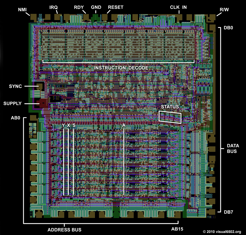
>This should help...: >http://visual6502.org/images/6502/6502_pad_annot_07.png . My >question is, and this may be off-topic, what is the device betwixt D3 and >D4?
I will study java script simulator later. I am not sure I understand your question "what is the device betwixt D3 and D4?" I think 3rd bit and 4th bit of data bus.
Bryan
I will study java script simulator later. I am not sure I understand your question "what is the device betwixt D3 and D4?" I think 3rd bit and 4th bit of data bus.
Bryan