6502.org Forum  Projects  Code  Documents  Tools  Forum
It is currently Fri Nov 22, 2024 5:33 pm

All times are UTC


Post new topic Reply to topic  [ 297 posts ]  Go to page Previous  1 ... 13, 14, 15, 16, 17, 18, 19, 20  Next
Author Message
 Post subject:
PostPosted: Wed Sep 01, 2010 2:15 am 
Offline

Joined: Sat Jan 04, 2003 10:03 pm
Posts: 1706
The 6809 architecture is a wonderful CPU architecture; the 6303 is based on the 6809.

However, it's no 68000. ;)

Garth wrote:
Quote:
WDC could have put the '816 in a 48-pinner to avoid the need for the external '573 latch (which really is quite simple anyway).


Pins cost a lot of money, apparently. According to Chuck Moore, pin counts directly affect the costs of semiconductor fabrication runs. It appears non-linear as well.

Increasing from 40 to 48 pins could have placed the CPU outside the affordability window of prospective buyers.


Top
 Profile  
Reply with quote  
 Post subject:
PostPosted: Wed Sep 01, 2010 2:32 am 
Offline
User avatar

Joined: Fri Aug 30, 2002 1:09 am
Posts: 8543
Location: Southern California
Quote:
68xx is way ahead of 65xx.

The 6800 sure didn't run Forth as fast as the 6502 at a given clock speed, and the 6502 got to much higher clock speeds anyway through most of its history. The 6502 designers were ones that worked on the 6800 design at Mot and of course would not have made the '02 if they didn't think they could do better. But if you want to say 6809, then you have to compare to the 65816, which outperforms the 6809.

Quote:
Pins cost a lot of money, apparently. According to Chuck Moore, pin counts directly affect the costs of semiconductor fabrication runs.

I think the cost is in the testing, more than in just the pins themselves or the wire bonding.


Top
 Profile  
Reply with quote  
 Post subject:
PostPosted: Wed Sep 01, 2010 12:10 pm 
Offline

Joined: Mon Mar 02, 2009 7:27 pm
Posts: 3258
Location: NC, USA
Sorry guys, I was in one of those moods. Batty one might say, after banging my head against the wall all day. I was just talking trash, forgive me.

I realized this morning this whole idea of using a counter to manipulate CPU/RESet, EEPROM/OE and SRAM/OE and using software was a good idea when copying a small 8Kx8 EEPROM...

But if I want to copy the entire 512K EEPROM onto the 2Mx8 RAM, which would be a logical next step, I'm going to have to do it in hardware. Waiting for software to do this would just take too long. I can wire in the remaining address lines A0-A7 into the FPGA, and BE from the 6502. Then I can take control of everything related to EEPROM/SRAM and run the copy hardware at 2.5MHz. I hope it's that simple and I won't have to totally rewire the FPGA! I should have used a 144-pin XC2S100. BTW if you are looking for a nice "hidden" cache of FPGAs, try avnet.

I realize I may hit the same wall I'm at now trying to run from the SRAM, but this is the path I've chosen.

_________________
65Org16:https://github.com/ElEctric-EyE/verilog-6502


Top
 Profile  
Reply with quote  
 Post subject:
PostPosted: Wed Sep 01, 2010 11:46 pm 
Offline
User avatar

Joined: Fri Dec 11, 2009 3:50 pm
Posts: 3367
Location: Ontario, Canada
kc5tja wrote:
The 6809 architecture is a wonderful CPU architecture; the 6303 is based on the 6809.

However, it's no 68000. ;)

I think you mean the 6309 is based on the 6809 -- the numbers are somewhat confusing. I agree wholeheartedly that, like the 6809, the 6309 is a wonderful chip to code for (although still no 68000, as you say). 6809, 6309 and 68000 all far surpass the 6502's old nemisis, the 6800, which was a 1970's chip in the worst sense (as well as being lousy for Forth).

The 6309 (a Hitachi product) actually out-6809s the 6809, since it has additional registers and instructions (including some 32-bit operations). Moreover, the 6309 is faster than a 6809 running the same code at the same clock speed; this is because of internal improvements that result in fewer "dead cycles." This is an analogous comparison to that between certain 65xx chips: the 65CE02 is clock-for-clock faster than a 65C02 for the same reason.

-- Jeff
ps: 6809/6309 indirect-threaded NEXT is just two instructions!
Code:
LDX  ,Y++    ;Y is IP  X is W
JMP  [,X]


Top
 Profile  
Reply with quote  
 Post subject:
PostPosted: Thu Sep 02, 2010 6:39 am 
Offline
User avatar

Joined: Fri Dec 11, 2009 3:50 pm
Posts: 3367
Location: Ontario, Canada
ElEctric_EyE wrote:
if I want to copy the entire 512K EEPROM onto the 2Mx8 RAM, which would be a logical next step, I'm going to have to do it in hardware.

Certainly you'll need some hardware, because you're dealing with address spaces larger than the 65C02's 64K. But the ideal solution, I'd say, is to use the windowing (aka bank-switching) scheme you've already developed. (Instead it sounds like you're making extra work for yourself -- or maybe I've misunderstood). Anyway, how's this:

You've already arranged that your '02 has a 16K chunk ($4000-7FFF) of its address space that acts as a window into the bigger space, showing any 16K section as determined by the bank select register. By duplicating some circuitry it would be no great trick to have another bank register controlling another window at $C000-FFFF where the OS lives.

If your select registers were 8 bits wide, then 256 16K sections could be addressed. (This still fits with your undefined opcode idea.) It would give you a 4MB space that can be independently accessed through either window. 4MB is enough to hold your entire EEPROM and the entire SRAM, with no overlap or OE tricks required. (128 16K sections could map to the 2MB SRAM, and the EEPROM would easily fit in what's left.)

RESET would initialize the $C000-FFFF bank-register so that the EEPROM initially appears there. After reset, software takes over; I don't think I need to spell it out. Either window can point anywhere in either memory chip; you would copy from one window to the other. When you're done copying, you can map the (faster) SRAM into the $C000 window and leave it that way.

Just thinking out loud... :) Have you thought about application code for the PWA when it's finished? If you intend on using its generous allotment of memory, you'll need to get comfortable with windowing sooner or later. I guess I'm suggesting you start now.

-- Jeff


Top
 Profile  
Reply with quote  
 Post subject:
PostPosted: Thu Sep 02, 2010 7:21 am 
Offline

Joined: Mon Mar 02, 2009 7:27 pm
Posts: 3258
Location: NC, USA
No, I'm not abandoning the bank switching idea or the redefined opcode idea either. Just changing how I will go about copying the EEPROM to SRAM...
4MB? I might as well use all 8 bits of the register but it's going to depend on whether another IC can fit onto the 2.5"x3.8" board.
I posed a question on Xilinx forums and got a quick response from a nice fellow. I am going forward at this point with having PCB's made, after I design them of course. It'll be a few weeks at least. No need to have a finalized schematic, I'll just be sure to route ALL of the cpu pins to the FPGA and have a decent expandability connector... So I'm going with a 144 pin XC2S100E, which will have plenty of room to grow into!

_________________
65Org16:https://github.com/ElEctric-EyE/verilog-6502


Top
 Profile  
Reply with quote  
 Post subject:
PostPosted: Thu Sep 02, 2010 7:32 am 
Offline
User avatar

Joined: Fri Dec 11, 2009 3:50 pm
Posts: 3367
Location: Ontario, Canada
ElEctric_EyE wrote:
4MB? I might as well use all 8 bits of the register but it's going to depend on whether another IC can fit onto the 2.5"x3.8" board.
Isn't the register part of the FPGA? Could it be put there? Maybe I need to wait and see the schematic to understand.

Keep us posted!

-- Jeff


Top
 Profile  
Reply with quote  
 Post subject:
PostPosted: Thu Sep 02, 2010 7:44 am 
Offline

Joined: Mon Mar 02, 2009 7:27 pm
Posts: 3258
Location: NC, USA
Yes the register is inside the FPGA, presently an XC2S15, but I've run out of pins! Plus with a board with ground/power planes, I'll be eliminating 1 more variable. Noise! The SRAM is suckin some juice @275mA. And after all this testing I am having THE problem with the SRAM. The scope shows decent levels of noise @~30mV.

I've doubled my wirewrapping on all grounds on all 4 IC's (CPU, FPGA, EEPROM, & SRAM). I've lowered the frequency to the 4bit counter controlling the 6502/Res, EEPROM/OE, and SRAM/OE, so the software has more than 12 sec's to copy 16K($C000-$FFFF) from 512Kx8 EEPROM($7C000-$7FFFF) to 2Mx8 SRAM($1FC000-$1FFFFF). At the end of the copy software routine I have the STP($DB) command. Observing SYNC during the entire 12+sec's says that the software is never seeing the STP command....

I will devote the few hours I have left each workday mostly towards the new board layout. Yet some hours I will set aside on my days off (tue&wed) to still troubleshoot this problem as I hate unanswered questions.

_________________
65Org16:https://github.com/ElEctric-EyE/verilog-6502


Top
 Profile  
Reply with quote  
 Post subject:
PostPosted: Fri Sep 03, 2010 4:42 am 
Offline
User avatar

Joined: Fri Aug 30, 2002 1:09 am
Posts: 8543
Location: Southern California
Quote:
ps: 6809/6309 indirect-threaded NEXT is just two instructions!
Code:
LDX  ,Y++    ;Y is IP  X is W
JMP  [,X]

How many clocks? And what clock speed is available? I seem to remember the 6809 had some pretty long instructions, like 10 or 12 clocks, maybe more. Bruce gives a two-instruction indirect-threaded NEXT for the '816 here, which takes 11 clocks total. At 20MHz, that's 550ns. (The SuperCPU expansion for the Commodore 64 runs its 65816 at 20MHz.)


Top
 Profile  
Reply with quote  
 Post subject:
PostPosted: Tue Sep 07, 2010 7:02 pm 
Offline

Joined: Mon Mar 02, 2009 7:27 pm
Posts: 3258
Location: NC, USA
Spent almost 8 hours trying new troubleshooting angles. I'll keep it short and sweet.

Ohmed out each of the 54 pin TSOPII SRAM pins direct to the IC to negate bad soldering, or incorrect adapter spec's. No problem found.

Rechecked all wiring of the SRAM. No problem found.

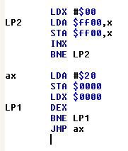
After many hours I started to focus on the copy software, and I tried to do a couple things... But my final little bit of software which finally did make itself onto the SRAM is below. I was able to run it @ 10MHz.

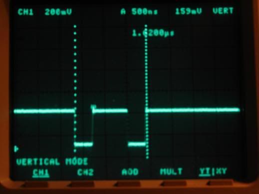
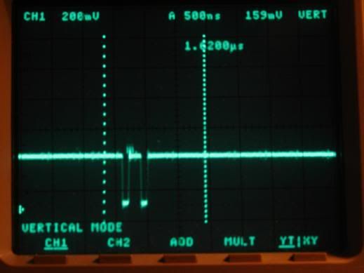
I was scoping out one of the MUX'd upper address lines (A14-A20), namely A14, since right now they are all hardwired to switch all low or all high. When running at EEPROM copy speed 2.5MHz, I saw a simple repetitive pattern. At 10MHz, I saw confirmation of the same pattern.

My problem is in the bank switching I know now. It is switching as shown below, but the timing must be off. It's not reading $0000 correctly. The scope pattern never changes when I try to lengthen or shorten the loop reading from $0000. For now I rest. Tomorrow a new day!

Image

Banked A14 running from 200ns EEPROM, cpu@2.5MHz:
Image

Banked A14 running from 10ns SRAM, cpu@10MHz:
Image

_________________
65Org16:https://github.com/ElEctric-EyE/verilog-6502


Top
 Profile  
Reply with quote  
 Post subject:
PostPosted: Tue Sep 07, 2010 8:16 pm 
Offline

Joined: Mon Mar 02, 2009 7:27 pm
Posts: 3258
Location: NC, USA
Not sure how reliable but it is running @20MHz from SRAM CPU @3.3V! If it runs @40MHz, I'll know if I've got issues. BRB

No luck @40MHz, thank you Jesus!

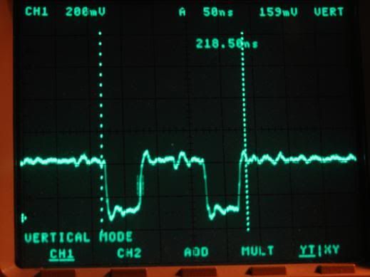
Granted it is a simple program, no ALU testing etc. But my address decode signals are good to that speed! I am using RWB with phase 2 to decode SRAM _WE

same as previous post but CPU @20MHz, and resized scope cursors for more accurate measurement. (not too accurate, I was too excited. I usually try to measure a square wave from "mid way lo to high on the rising edge" to "mid way high to low falling edge". This pic shows I was clearly off. Nonetheless the CPU was running)
Image

EDIT #2: Added pic, and added how I measure, refixed measure.

_________________
65Org16:https://github.com/ElEctric-EyE/verilog-6502


Last edited by ElEctric_EyE on Tue Sep 07, 2010 9:03 pm, edited 3 times in total.

Top
 Profile  
Reply with quote  
 Post subject:
PostPosted: Tue Sep 07, 2010 8:32 pm 
Offline

Joined: Tue Jul 05, 2005 7:08 pm
Posts: 1043
Location: near Heidelberg, Germany
ElEctric_EyE wrote:
My problem is in the bank switching I know now. It is switching as shown below, but the timing must be off. It's not reading $0000 correctly. The scope pattern never changes when I try to lengthen or shorten the loop reading from $0000. For now I rest. Tomorrow a new day!


As far as I understand it you're scoping the time between the STA $0000 and the LDA $0000: a write, three reads in ROM, and a read. What you're not measuring is the time for the actual loop, as the loop happens in the part that's "off-screen" on your scope.

Actually ... at 2.5MHz, 5 cycles should be 5 times 400ns, i.e. 2us, not 1600ns. It actually looks like you're measuring 4 cycles, two RAM accesses with 2 other accesses between them.

Anyway, try to increase the time base to include the loop. A loop with 32 iterations is about 160 cycles, which at 2.5MHz makes about 65us (or about 16us for 10MHz). Both times, 65us resp. 16us are too long for the scope setting in the included pictures. If you increase the time base to show at least one full iteration, you can then decide whether the loop works or not.

One thing that people sometimes do is to use an "EA" simulator. put the CPU in an adapter, and connect the data bus fixed to "EA" (disconnect IRQ, NMI, maybe use r/-w to qualify). The CPU then counts through all addresses (two cycles for each address) and you can more easily scope the repetitive signals on the address lines. Haven't tried that yet ... (at least in hardware. My VHDL test actually uses this method :-)

Personally, I have an adapter to plug into the CPU socket, where I can statically set the address bus of the CPU and check the address decoding easily. Even includes a jumper for the r/-w and a push button for phi2 :-) That's a very crude CPU simulator, but might work.

On a side note...: Recently I have used a 65816 board, plugged into the 6502 socket of a Commodore PET4032, that runs in the board's RAM and ROM. So I can use decent test programs loaded via the PET's I/O to test the actual behavior of the (broken) 4032. Thinking about it, even earlier (in the 90ties) I have actually used my CPU emulator board for my CS/A computer to replace the CPU of a VC1541. The VC1541's memory just became a 64k window in the 1MB CS/A memory. I could replace and test ROMs for example. I didn't have to fix the VC1541 then though.

Hope that helps,
André

Top
 Profile  
Reply with quote  
 Post subject:
PostPosted: Tue Sep 07, 2010 9:00 pm 
Offline

Joined: Mon Mar 02, 2009 7:27 pm
Posts: 3258
Location: NC, USA
fachat wrote:
... A loop with 32 iterations is about 160 cycles, which at 2.5MHz makes about 65us (or about 16us for 10MHz)...


Thanks for calculating that Andre. I have checked the "entire" loop. Difficult to measure since the spikes are very narrow, but @20MHz I measure about 8uS. OH jeez, so now I need to change the loop variable and recheck. Thank you! BRB

I changed from #$20 to #$10, no change. I'll have to experiment more tomorrow.

_________________
65Org16:https://github.com/ElEctric-EyE/verilog-6502


Last edited by ElEctric_EyE on Tue Sep 07, 2010 9:25 pm, edited 1 time in total.

Top
 Profile  
Reply with quote  
 Post subject:
PostPosted: Tue Sep 07, 2010 9:25 pm 
Offline

Joined: Tue Jul 05, 2005 7:08 pm
Posts: 1043
Location: near Heidelberg, Germany
ElEctric_EyE wrote:
same as previous post but CPU @20MHz, and resized scope cursors for more accurate measurement. (not too accurate, I was too excited. I usually try to measure a square wave from "mid way lo to high on the rising edge" to "mid way high to low falling edge". This pic shows I was clearly off. Nonetheless the CPU was running)


Even more, 200ns make 4 cycles @20MHz (cycle time 50ns). Maybe you should check whether your assembler optimized the "LDA $0000" to "LDA $00", i.e. from absolute to zeropage addressing. That would explain the 4 cycles:
Code:
0:   write $00
1:   read opcode "LDA_ZP"
2:   read parameter address "$00"
3:   read address $00


You should recalculate the loop timing with this in mind.

André


Top
 Profile  
Reply with quote  
 Post subject:
PostPosted: Wed Sep 08, 2010 4:21 pm 
Offline

Joined: Mon Mar 02, 2009 7:27 pm
Posts: 3258
Location: NC, USA
Brainfog is my problem. Like a long distance runner finally hitting the finish line, saying to himself I made it but so tired. I'm like that, but I still push on even further and I get brainfog. I'll explain, and Andre helped me in the brainfog moment.

The double dips in all the scope pics are the LDA $0000 and STA $0000 since I am scoping out the upper address lines going to the SRAM (A14-A20). My brainfog moment was incorrectly concentrating on the delay in between when they go low. I was busy on top speed measurements, and being so excited that I had finally had something working, I was focusing on the actual waveforms, not what was really going on.

Now I am correctly focusing NOT on the delay between the STA $0000 and LDX $0000, BUT ON THE DELAY BETWEEN LDX $0000 AND STA $0000. And @20MHz, this morning I found out it is indeed reading from $0000 correctly. As I can see on the scope, the time between both "double dips" is changing consistently when changing the value in $0000.

A few more tests/re-tests and I think I'll have it.

Edit: edited observations, added CAP's.

_________________
65Org16:https://github.com/ElEctric-EyE/verilog-6502


Last edited by ElEctric_EyE on Fri Sep 17, 2010 2:09 am, edited 1 time in total.

Top
 Profile  
Reply with quote  
Display posts from previous:  Sort by  
Post new topic Reply to topic  [ 297 posts ]  Go to page Previous  1 ... 13, 14, 15, 16, 17, 18, 19, 20  Next

All times are UTC


Who is online

Users browsing this forum: No registered users and 31 guests


You cannot post new topics in this forum
You cannot reply to topics in this forum
You cannot edit your posts in this forum
You cannot delete your posts in this forum
You cannot post attachments in this forum

Search for:
Jump to: