6502.org Forum  Projects  Code  Documents  Tools  Forum
It is currently Fri Jun 28, 2024 10:09 pm

All times are UTC


Post new topic Reply to topic  [ 297 posts ]  Go to page Previous  1 ... 9, 10, 11, 12, 13, 14, 15 ... 20  Next
Author Message
 Post subject:
PostPosted: Fri Apr 16, 2010 1:10 am 
Offline

Joined: Mon Mar 02, 2009 7:27 pm
Posts: 3258
Location: NC, USA
OwenS wrote:
...By the way, are you sure you're supposed to be running the clock to the clock enable pin, and the enable to the clock pin?


I was wondering if someone would pick that up. An honest mistake. I had read the post on the Xilinx forums and tried to wire up the circuit by memory, and I realized after I posted then double checked my circuit, that I had McGett's suggestion backwards (as related to the clock and enable signals), as you pointed out. The way I have it posted above works. I'll try it as suggested and see if it works as well. I've been too busy trying to figure out a circuit that I can read from as well as write too... An AND gate you'd think even if there is a O2 clock gated through it would work, like you said though, there's the jitter factor. I associate jitter with analog circuits like VCO's not purely digital circuits...

_________________
65Org16:https://github.com/ElEctric-EyE/verilog-6502


Top
 Profile  
Reply with quote  
 Post subject:
PostPosted: Fri Apr 16, 2010 1:41 am 
Offline

Joined: Thu Jul 26, 2007 4:46 pm
Posts: 105
I suppose jitter was not the correct word; it would probably have been waveform cutting?

In any case, I'm referring to when the enable logic could force the clock low part way through a high period (or release it during a corresponding time) and therefore cause the timing constraints to be violated. The device's enable logic will, of course, be designed to handle CE being asserted/deasserted at any point and synchronize the clock internally


Top
 Profile  
Reply with quote  
 Post subject:
PostPosted: Sat Apr 17, 2010 2:32 am 
Offline

Joined: Mon Mar 02, 2009 7:27 pm
Posts: 3258
Location: NC, USA
I'm gonna ramble here a little, forgive me as the hobbyist I am, maybe out of his league?

Waveform cutting, I can understand that... (Please noone take the following in a negative light), but...

I think with this project here (I am hoping, I am not intimidated by logic), I will finally have to conquer the timing diag's... I never claimed to be a pro but I want to be. There are several hobbyists here in this forum, that should be Pro's IMHO, and I for one thank them for their contribution and offers to help and their posts...

I'm done rambling now. I just got home from work, I hope I don't regret reading my words here, as sometimes I have in the past that I have written.

But, I may need a rest for a couple weeks, in order to get a fresh perspective. Maybe read some 6502/CPLD manuals. Just read some instead of diving in head on and posting so much...

_________________
65Org16:https://github.com/ElEctric-EyE/verilog-6502


Top
 Profile  
Reply with quote  
 Post subject:
PostPosted: Sat Apr 17, 2010 3:57 am 
Offline
User avatar

Joined: Fri Aug 30, 2002 9:02 pm
Posts: 1696
Location: Sacramento, CA
What you are going through happened to me during the SBC-3 and 65SPI development. I woudl smash ahead until I hit a road block, spend lots of time trying to bust through it, then fall back and regroup.

The SBC-3 concept actually started back in 2005 but after 6 months, I put it away until 2007. Even then, it took two more years to get it completed.

Your project, like mine, is big and requires a lot of thought and if/then iterations.

With your determination, I'm sure you will see a successful outcome when the time is right.

Good luck!

Daryl


Top
 Profile  
Reply with quote  
 Post subject:
PostPosted: Tue May 04, 2010 5:23 pm 
Offline

Joined: Mon Mar 02, 2009 7:27 pm
Posts: 3258
Location: NC, USA
Thanks for the moto (motivation) 8bit!. More patience/troubleshooting was needed on my part.

Got the A14-A18 bank address port to work bidirectional with some help from here ( 
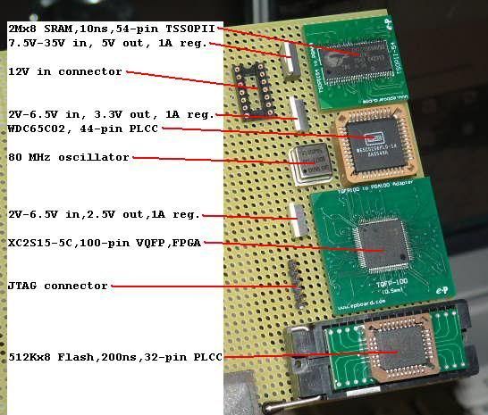
viewtopic.php?t=1572 ) , so now I can just do an INC on the register itself. In testing, I was using a memory location to R/W from, then write the register data which is many more cycles stolen from updating pixel data... The whole system is running now @ a conservative 7MHz in SRAM mode after reading from the slow EEPROMs.

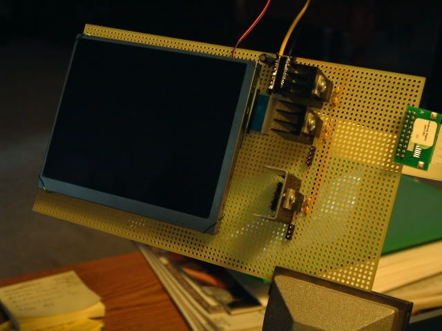
The display is what is really holding me up as far as pushing CPU speeds above 10MHz. So that priority is on the backburner ATM until I get the 50MHz 640x480 display in June...

In the meantime, I've been working on another CPLD that has: a 16-bit counter, 2 8-bit latches for the CPU interface, and address decoding. Originally I intended the PW counter frequency to be variable, but after getting into the design, I realized I needed a steady time base to work from so the CPU can "know" the length of each pulse width based on the result of the 16-bit counter, and base it on seconds...

Anticipated injector pulse widths on a 5.7L engine, with added margins, are 1mS to 20mS according to this wiki ( http://en.wikipedia.org/wiki/Fuel_injection ) for a 5.0L engine. A 16-bit counter with an active high enable time of 20 mS will reach a terminal count at 3.3 MHz (1/.020x65536). Well below any speed constraints of the CPLD.

For Sh*ts and giggles I fitted another 16-bit counter acting as a divider, a 16-bit MUX, and a 4 bit readable port to control frequency into the first counter. The 16-bit MUX does "max" out the CPLD resources very quickly, now at 98%... Using an 80MHz osc, I'll have a 16-bit range from 40MHz - 1.2kHz, that can measure pulse widths down to about 1.6uS. This will throw in a monkey wrench for that "known" timebase, I'll have to figure that out later.

A Terminal Count signal of the PW counter will go to /NMI, this will run a simple subroutine to INC the 4-bit port to speed up the frequency.

Just need to wire in the new CPLD and oscillator... And rewire JTAG for 2 CPLDs.

_________________
65Org16:https://github.com/ElEctric-EyE/verilog-6502


Top
 Profile  
Reply with quote  
 Post subject:
PostPosted: Fri May 28, 2010 3:01 am 
Offline

Joined: Mon Mar 02, 2009 7:27 pm
Posts: 3258
Location: NC, USA
Yesterday, I finally got the main 80MHz 16-bit frequency divider, 16-bit MUX, and the 16-bit PW counter, and control logic for the MUX working. After trying to fit the interface 8-bit latches and tristate buffers for the PW counter, the design wouldn't fit onto the CPLD. This being the 2nd CPLD. 74 macrocells needed on a 72 macrocell CPLD. So close, but I couldn't make it fit...( http://forums.xilinx.com/t5/Implementat ... td-p/71687 )

Now looking into possibly using an FPGA, a dead family of FPGA, to fit both CPLD designs into one single IC... The 5v tolerant Spartan 2. No longer produced, but still sold. The last of the 5v I/O tolerant FPGAs. I would have to use an older version of ISE, but that's ok... DigiKey still selling the Spartan 2's in 100 TQFP version for <$10 each... This will be the 3rd "iteration" of this project, i.e. a total rewiring from scratch. This will be the final iteration I promise. I am anxious to end it, and focus next on custom opcodes. Soon (in June) I am expecting the 640x480 display and plan to use it in this final phase.

_________________
65Org16:https://github.com/ElEctric-EyE/verilog-6502


Last edited by ElEctric_EyE on Wed Jun 02, 2010 3:41 pm, edited 1 time in total.

Top
 Profile  
Reply with quote  
 Post subject:
PostPosted: Tue Jun 01, 2010 5:53 pm 
Offline

Joined: Mon Mar 02, 2009 7:27 pm
Posts: 3258
Location: NC, USA
A little more research led me to the Coolrunner II XPLA3 series of CPLD's, the 5V I/O tolerant series. I was able to fit my last design that would barely not fit onto a 72 macrocell XC9572, onto a 64 macrocell CoolRunner XPLA3 CPLD, the XCR3064. Currently pursuing either a 9ns 100-pin VQFP XCR3128 (CoolRunner II XPLA3 CPLD) or a 5ns XC2S15-5VQG100C (Spartan II FPGA). One 100-pin VQFP to BGA adapter socket will fit one of these two. We'll see what the ISE software decides...

_________________
65Org16:https://github.com/ElEctric-EyE/verilog-6502


Top
 Profile  
Reply with quote  
 Post subject:
PostPosted: Wed Jun 16, 2010 7:10 pm 
Offline

Joined: Mon Mar 02, 2009 7:27 pm
Posts: 3258
Location: NC, USA
Well I went with the Spartan 2, and system voltage will be at 3.3V. The single most limiting factor on deciding on an operating voltage for this final stage, was the speed of the largest SRAM I could find. Large/Fast SRAM is top prioity for this last stage. I found 2Mx8 SRAM only in 3.3V. At 5V, the largest I found was 512Kx8. (The cost was $8 for the 512K part, and ~$40 for the 2M part. Quite a difference, but I am thinking ahead to very limited board space when it comes time to have boards prefab'd.)

Before, operating voltage was priority only because of the (incorrectly assumed on my part) limitations of my EEPROM programmer. I am now aware that it can burn a 3.3V device. This is the other reason I decided to make the whole system 3.3V. Although, this will limit the WDC65C02 to 14MHz...

Final speed of the CPU will depend on the max operating speed the Spartan 2. I am tapping the main Pulse Width 16-bit counter inside the FPGA for the CPU clock. I am shooting for a 12.5MHz CPU clock if the FPGA can run @100MHz. If it can't run that fast, I'll have to settle for 80MHz, and a 10MHz CPU. Either way, the Spartan 2 will be running 8x faster than the CPU and I think there will be alot of room for some interesting possibilities...

I am going to try some custom opcodes to address the 2Mx8 SRAM and 512Kx8 EEPROM. Instead of an LDA/STA to bank registers, 2 "unused" opcodes will be "read" into the bank flip flops using the: SYNC signal, an 8-bit magnitude comparator, and the Phase 2 Signal to control a 2-bit counter. Thanks to Dr. Jefyll for his help on his thread here: viewtopic.php?t=1556, all detailed info about my use of mod'd opcodes will be posted there.

I am currently in the process of re-inputting the schematic for the FPGA. Here within the next couple weeks, I hope to have something working.

(In hindsight, now that the system is @ 3.3V, I maybe should have used the current Spartan 3 family in 100-pin VQFP... Still, the Spartan 2 is 5V I/O tolerant. It may be useful for something in the future...)

Here is what I have assembled so far in this, the last! chapter:

Image

_________________
65Org16:https://github.com/ElEctric-EyE/verilog-6502


Top
 Profile  
Reply with quote  
 Post subject:
PostPosted: Sat Jun 26, 2010 1:34 am 
Offline

Joined: Mon Mar 02, 2009 7:27 pm
Posts: 3258
Location: NC, USA
The backordered 5.7" 640x480 TFT display is finally on it's way. It's going to change quite a bit of my current software. (I'm starting to get a feeling like I'm changing too many variables for this new build... Gonna be a challenge thats for sure!) Addressing scheme is the same as with the old unit, even though this one has more functions. Hardware windows, being one of them, if I remember correctly... Same price I paid for the now discontinued 320x240 8-bit display last year. If this is the price of progress, it is worth it.

Link for the display here: http://www.newhavendisplay.com/index.ph ... 9ekbsgp5m3

Edit:
ElEctric_EyE wrote:
... The 5v tolerant Spartan 2. No longer produced, but still sold. The last of the 5v I/O tolerant FPGAs...

In the previous post I stated there was only 1 family of 5V tolerant FPGA made by Xilinx. That's what I knew then, this is what I have learned now: According to this new Xilinx thread (look down to the 5th post), the original Virtex series is also 5V I/O tolerant.
http://forums.xilinx.com/t5/Spartan-Fam ... td-p/74303

Unable to find any versions available on Digi-Key no matter which version or # of pins of Virtex family ( http://www.xilinx.com/support/documenta ... /ds003.pdf)

_________________
65Org16:https://github.com/ElEctric-EyE/verilog-6502


Top
 Profile  
Reply with quote  
 Post subject:
PostPosted: Wed Jun 30, 2010 8:47 pm 
Offline

Joined: Mon Mar 02, 2009 7:27 pm
Posts: 3258
Location: NC, USA
Virtex 2 would probably be a nice choice for a 6502 on FPGA, since no logic level converters are needed... Although, I can't find any!

I received the new NHD 5.7" 640x480 display yesterday, so I was able to finalize socket positions and start wiring it up. Today I completed wiring: the 12V-in connector, the 5V, 3.3V, and the 2.5V regulators. The heat sinks are from old circuit boards. They may be overkill, but I prefer large safety margins. The 12V-in connector feeds the 5V regulator. The 5V reg feeds the 3.3V AND the 2.5V regulators. All tested OK...

Next step is bypass cap's and power connections to all IC's...

Like the last display unit I received from NHD, it is factory jumper selected for an 8080 style interface. The soldered jumper is easily changeable to 6800 style interface as shown here thanks to NHD: http://www.newhavendisplay.com/forum/vi ... ?f=6&t=356

Question: Should I stay with .1uF bypass cap's? I've seen the formula's saying to use bypass cap's in the nF range. I'm not comfortable with that. I can see maybe .05uF, instead of the .1uF I have been using.

A pic of what has been assembled so far:
Image

EDIT: Grammar, spelling.

_________________
65Org16:https://github.com/ElEctric-EyE/verilog-6502


Last edited by ElEctric_EyE on Thu Jul 01, 2010 12:47 am, edited 2 times in total.

Top
 Profile  
Reply with quote  
 Post subject:
PostPosted: Wed Jun 30, 2010 8:54 pm 
Offline

Joined: Sat Jan 04, 2003 10:03 pm
Posts: 1706
ElEctric_EyE wrote:
Virtex 2 would probably be a nice choice for a 6502 on FPGA, since no logic level converters are needed... Although, I can't find any!


This is the problem with the FPGA industry as a whole. Once an FPGA becomes cheap enough to fall into amateur hands, they discontinue the architecture, we're forced to grovel for scraps. It wouldn't be so bad, though, if FPGA vendors would agree on a wire standard for programming not only current devices but future devices as well. But, no, they can't let out any "trade secrets."

This is why I support Intellasys and GreenArrays chips so much. I really hope they can bring chips to the mass market, so that we can hack with general purpose, long-lived hardware instead of the poster-children of planned obsolescence.

Yes, while slower than FPGAs, they're plenty fast enough to drive a VGA entirely in software at 640x480, if not 800x600 with tricky programming.


Top
 Profile  
Reply with quote  
 Post subject:
PostPosted: Wed Jun 30, 2010 9:56 pm 
Offline
User avatar

Joined: Fri Aug 30, 2002 1:09 am
Posts: 8460
Location: Southern California
Quote:
Question: Should I stay with .1uF bypass cap's? I've seen the formula's saying to use bypass cap's in the nF range. I'm not comfortable with that. I can see maybe .05uF, instead of the .1uF I have been using.

If capacitors were perfect and you did not have significant stray inductance, then .1µF would always be better for bypassing than .01µF. Common hobbyists' projects typically have a lot more stray inductance (mostly from lead length) than SMT production stuff though, so they'll get better high-frequency bypassing with the .01µF. In many cases, if you want to increase the capacitance, you'll do better putting a few .01's in parallel than using a .1µF. There was some discussion of that here.


Top
 Profile  
Reply with quote  
 Post subject:
PostPosted: Wed Jun 30, 2010 10:19 pm 
Offline

Joined: Thu Jul 26, 2007 4:46 pm
Posts: 105
kc5tja wrote:
ElEctric_EyE wrote:
Virtex 2 would probably be a nice choice for a 6502 on FPGA, since no logic level converters are needed... Although, I can't find any!


This is the problem with the FPGA industry as a whole. Once an FPGA becomes cheap enough to fall into amateur hands, they discontinue the architecture, we're forced to grovel for scraps. It wouldn't be so bad, though, if FPGA vendors would agree on a wire standard for programming not only current devices but future devices as well. But, no, they can't let out any "trade secrets."

You can pick up a Virtex II at digikey for about $80 for the smallest chip. Thats not bad for a Virtex - you're really looking at the wrong family; the VIIs are approaching discontinuation and are old devices. They're really intended for building high performance, low quantity, high cost equipment - think network switches and such. The more expensive ones (Up to $4000 per chip) are generally rarely found outside development boards (They're often used for CPU design).

If you want an FPGA family to use for your own designs, look at the Spartan III (or Altera's alternative). They're the volume families, built in more modern processes and cheaper to produce. Of course, they don't have 5V IO - the process nodes which support them economically simply can't support it.

Quote:
This is why I support Intellasys and GreenArrays chips so much. I really hope they can bring chips to the mass market, so that we can hack with general purpose, long-lived hardware instead of the poster-children of planned obsolescence.

Planned obsolecesence? The Virtex II family is over 10 years old. That's a very good life span for a device of this complexity. Processes get discontinued, and Xilinx aren't at liberty to choose when (no fabless company is).

Oh, and the programming information for Xilinx devices is very well documented. The open source OpenOCD JTAG system knows how to program them; as does the free ISE software.

Quote:
Yes, while slower than FPGAs, they're plenty fast enough to drive a VGA entirely in software at 640x480, if not 800x600 with tricky programming.


Tell me: If I program that for a GreenArrays device, how do I move it to one by another vendor?

Because, with an FPGA, all I do is recompile it with their software. The language is standard. Heck; most of the time even the programming cables are standard (and, indeed, via OpenOCD you can use the same cable to program your FPGAs, CPLDs and ARM CPUs - and all through the same board connector)


Top
 Profile  
Reply with quote  
 Post subject:
PostPosted: Thu Jul 01, 2010 4:40 pm 
Offline

Joined: Sat Jan 04, 2003 10:03 pm
Posts: 1706
OwenS wrote:
Oh, and the programming information for Xilinx devices is very well documented.


The last I looked, I was completely unable to find documentation on the bitstream format used to program Xilinx's devices. E.g., there is no information with which I could use to enhance Icarus to support synthesis for the newer FPGAs, or to create my own completely new logic design tool.

Quote:
The open source OpenOCD JTAG system knows how to program them; as does the free ISE software.


The JTAG interface standards cover bus protocol, which of course is well documented. It's what you communicate over that bus protocol that I'm talking about.

Quote:
Tell me: If I program that for a GreenArrays device, how do I move it to one by another vendor?


The GA device is a matrix of Von Neumann-architecture microprocessors, so you'll need to recompile your code for the new device's microprocessors (just as you need to recompile your Verilog for new FPGAs). Then, you'll need to program the chip through a cable or embed the source in an SPI-compatible EEPROM device.

The nice thing about GA's chips is you can talk to them via either RS-232 or SPI, depending on which core you choose to boot the chip with. The bit-stream is fully documented -- you're just downloading a raw binary image of an instruction stream into a region of RAM.

Quote:
The language is standard.


SQL is standard too, and yet applications invariably find themselves vendor-locked. I've talked with the author of Icarus on the gEDA mailing lists in the past, and he'll be the first to tell you that Icarus doesn't simulate all Verilog designs out there because of tons of vendor-specific inclusions or interpretations of the "standard".

While I don't doubt things are way better than they were when I last looked, it's by no means a completely solved problem.


Top
 Profile  
Reply with quote  
 Post subject:
PostPosted: Thu Jul 01, 2010 9:52 pm 
Offline

Joined: Thu Jul 26, 2007 4:46 pm
Posts: 105
kc5tja wrote:
OwenS wrote:
Oh, and the programming information for Xilinx devices is very well documented.


The last I looked, I was completely unable to find documentation on the bitstream format used to program Xilinx's devices. E.g., there is no information with which I could use to enhance Icarus to support synthesis for the newer FPGAs, or to create my own completely new logic design tool.

I can't say I know the specifics of the bitstream format; that changes per device since its really just a dump of the device's configuration RAM and therefore unstructured.

Quote:
Quote:
The open source OpenOCD JTAG system knows how to program them; as does the free ISE software.


The JTAG interface standards cover bus protocol, which of course is well documented. It's what you communicate over that bus protocol that I'm talking about.

The commands for downloading bitstreams to the device are documented. As said, OpenOCD can download to Xilinx FPGAs.

Quote:
Quote:
Tell me: If I program that for a GreenArrays device, how do I move it to one by another vendor?


The GA device is a matrix of Von Neumann-architecture microprocessors, so you'll need to recompile your code for the new device's microprocessors (just as you need to recompile your Verilog for new FPGAs). Then, you'll need to program the chip through a cable or embed the source in an SPI-compatible EEPROM device.

The nice thing about GA's chips is you can talk to them via either RS-232 or SPI, depending on which core you choose to boot the chip with. The bit-stream is fully documented -- you're just downloading a raw binary image of an instruction stream into a region of RAM.

Where on their website is this instruction set documented? Heck, where are the datasheets?

Where do I get a standard toolchain for the device? (In the case of an MCU, the de facto standard toolchain would undoubtedly be a C compiler & linker)

Quote:
Quote:
The language is standard.


SQL is standard too, and yet applications invariably find themselves vendor-locked. I've talked with the author of Icarus on the gEDA mailing lists in the past, and he'll be the first to tell you that Icarus doesn't simulate all Verilog designs out there because of tons of vendor-specific inclusions or interpretations of the "standard".

While I don't doubt things are way better than they were when I last looked, it's by no means a completely solved problem.


While there are deviations - as there are for all multi-vendor standards - in general it is possible to write a portable design. Most of the vendor-specific stuff is so documented, and primarily there to allow you to optimize (E.G. blockram or multiplier primitives)


Top
 Profile  
Reply with quote  
Display posts from previous:  Sort by  
Post new topic Reply to topic  [ 297 posts ]  Go to page Previous  1 ... 9, 10, 11, 12, 13, 14, 15 ... 20  Next

All times are UTC


Who is online

Users browsing this forum: No registered users and 0 guests


You cannot post new topics in this forum
You cannot reply to topics in this forum
You cannot edit your posts in this forum
You cannot delete your posts in this forum
You cannot post attachments in this forum

Search for:
Jump to: