Excellent info, thank you for the quick response! What you have mentioned is alot for my small brain to absorb...
Right now I (think?) I understand a few things:
1) It is possible to address up to 16MB contiguously, and have a JSR/RTS cross page boundaries automatically? (I DO need to re-re-re-read your webpage about this issue to fully understand how it works.). But, is this what you were referring to in your last paragraph of your last post?
2) I do know the signals I will need for the FPGA.
3) I will have to check the details between Rockwell's and Western Design Center's 6502's NOP's.
Thanks for your help. I am at the "if we see, we remember" stage. Soon I will be at the "if we do, we understand stage" and be able to add positive feedback hopefully.
early Interrupt Acknowledge. Defining unused opcodes.
-
ElEctric_EyE
- Posts: 3260
- Joined: 02 Mar 2009
- Location: OH, USA

ElEctric_EyE wrote:
is this what you were referring to in your last paragraph of your last post?
I'd better double-check that we're talking about the same thing! I visualize your window as occupying (say) addresses 8000 to C000 hex. By altering the contents of your circuit's "Window Select Register" -- I just made up that name, btw -- you could cause various 16K chunks of your humongous EEPROM/ram/whatever to appear at 8000 - C000. If the WSR is 8 bits wide then that would allow you to select between as many as 256 different different chunks, for a grand total well beyond the 65C02's usual 64K addressing limit. (The same trick was popular at one time for PCs. Known by the Marketing term "Expanded Memory," it allowed 8088 CPUs to transcend their usual 1 MB addressing limit.)
As for a means to update the WSR (so that different chunks may be selected), the conventional technique is to simply assign it an address that memory-address decoding circuitry will recognize. Then the update becomes a simple matter of the program writing from a CPU register to the WSR's address. In other words, just an ordinary output port. (The updated value is stored immediately in the WSR latch/flip-flop. But the stored value isn't used except when 8000 - C000 addresses appears on the address bus. C000 - 8000 addresses are what cue your hardware, indicating cycle-by-cycle whether or not the current access should be treated as part of the window.)
If what I've just described is comfortably within your capabilities then you can progress to the fancier approach of defining a new opcode capable of performing the update. But the fancy approach doesn't offer any earth-shattering advantage; writing to an I/O address is still a perfectly acceptable solution. (What is a big advantage is being able to juggle windows which are a full 64K in size. KK manages this, but at a cost in terms of complexity. Since the window is 64K in size, that means the CPU address bus is now useless for telling you whether or not to treat any given bus cycle as part of the window! Instead, microcode or other means are needed to make that window/not-window decision every cycle.)
Remember that your circuit must allow the regions not in the window (the regions 0 - 8000 and C000 - FFFF) to remain fixed, so that stuff like your stack, Zero Page and the interrupt vectors doesn't disappear! Reiterating, the WSR comes into play only on cycles during which the CPU produces addresses that fall within the window. BTW you'll notice that none of this requires that your CPLD be clocked faster than the CPU clock rate. Have fun, & bye for now
[Edit: clarity; remarks re cycle-by-cycle timing]
Last edited by Dr Jefyll on Mon Jun 07, 2010 1:51 pm, edited 1 time in total.
-
ElEctric_EyE
- Posts: 3260
- Joined: 02 Mar 2009
- Location: OH, USA
OK, didn't mean to keep raising new topics... For now my goal will be to do a simple data bus "snoop" for one of the undefined NOP's, and then for the following data to be written into the 7 bit bank register, which controls A14-A20. (maybe 8 bits for 2x(4Mx8), since decoding will require just one more inverter)
I still plan to incorporate the EEPROM to SRAM COPY so the 65C02 can run as fast as possible. I was hoping for 5V operation. The FMax vs VDD says at 5V to expect around 20MHz. Unfortunately for me, large/fast SRAM's do not run at these voltages. So, everything will be running at 3.3V, limiting speed of the CPU to 14MHz.
Off for a couple weeks to wire-up a new design using...:
1 5nS Spartan 2 FPGA
1 WDC65C02, ??>10MHz
1 2Mx8, 10nS Asynchronous SRAM
1 512Kx8, 150nS EEPROM
1 80MHz Crystal
1 640x480 pixel, 65K color TFT display
After a little experimentation, I'll pose some valid questions. Thanks again Dr. Jefyll!
-
ElEctric_EyE
- Posts: 3260
- Joined: 02 Mar 2009
- Location: OH, USA
Dr Jefyll wrote:
... I visualize your window as occupying (say) addresses 8000 to C000 hex.
ElEctric_EyE wrote:
...Right now I (think?) I understand a few things:
1) It is possible to address up to 16MB contiguously, and have a JSR/RTS cross page boundaries automatically?
1) It is possible to address up to 16MB contiguously, and have a JSR/RTS cross page boundaries automatically?
Dr Jefyll wrote:
ElEctric_EyE wrote:
is this what you were referring to in your last paragraph of your last post?
-
ElEctric_EyE
- Posts: 3260
- Joined: 02 Mar 2009
- Location: OH, USA
ElEctric_EyE wrote:
Yes, $8000-$BFFF, the largest chunk of memory to decode easily...
Quote:
your webpage [...] why I assumed this
Last edited by Dr Jefyll on Wed Jun 09, 2010 7:21 pm, edited 1 time in total.
I wrote:
none of this requires that your CPLD be clocked faster than the CPU clock rate
So, your CPLD doesn't need to be clocked faster than the CPU clock rate in order to use undefined opcodes. Of course, for your particular project there may be other signals/issues that call for faster clocking.
[Edit: other KK-like features you don't need include op-code substitution (because 1 new op is easier to map than 44) and microcode (because, with a less-than-64K window, you can rely on the address bus to tell you which bus accesses to treat as "window").]
I finally finished reading your (rather lengthy) Pulse Width Analyzer thread, and it all seems solid. I expect you'll soon have this windowing thing adapted to use an undefined opcode and humming like a top
-
ElEctric_EyE
- Posts: 3260
- Joined: 02 Mar 2009
- Location: OH, USA
I've finally wired everything up... The memory map is here:
viewtopic.php?t=1370&start=190 , I divided the 64K into 16K blocks to keep it simple.
The address decoding scheme I'm using is logical but isn't working. I'm failing to understand why, but I think I know, in part because I am bad with timing diag's. So let me thank anyone ahead of time for any help they can offer!
The first piece of software that runs, after a /Reset, copies $C000-$FFFF from EEPROM to SRAM using indirect indexed w/2 variables in zero page, so the multiplexers I'm using for A14-A20 at the 2M SRAM are switching from all zero's (for $0000-$3FFF) and all ones (for $C0000-$FFFF) when the program is running, and I'm thinking this is where my problem lies, but am unsure why.
Something is running, because I see the address and data lines switching on the 'scope...
Some facts:
The CPU is running at a conservative 2.5MHz since the access time for the EEPROM is 200ns.
Noise levels measure at different grounds are ~30mV, with everything running @3.3V. I don't think this is a problem. A concern though, since the
SRAM and display each take close to 300mA and everything is wirewrapped. Volts at each IC are in spec and clean looking.
I would like to know if I should pursue this idea further. Conceptually is it sound? or should I go on to another idea?
Last edited by ElEctric_EyE on Wed Aug 11, 2010 11:23 pm, edited 2 times in total.

Without seeing the actual decoding logic, or the init code, I will try to describe what I understand should be happening.
You say when the cpu addresses $C000-$FFFF, that SRAM is addressed to $1FC000-$1FFFFF.
Also, your ROM is addressed so that cput addresses $C000-$FFFF map to $7C000-$7FFFF in ROM.
Addresses in $0000-$3FFF always map to $000000-$003FFF in SRAM (for reads and writes presumably).
Do you have a control register in your CPLD that defines where reads come from vs. where writes go to, or are you using some other method?
After restart, your ROM must be mapped into Reads to address $C000-$FFFF or else your startup code will never run. If Reads are coming from SRAM, then you are most likely executing invalid code from uninitialized SRAM.
I would guess that if you can map writes into RAM while reading from ROM, that a simple
sequence would move ROM to RAM, then writing to a control register to set Reads from RAM vs. ROM, would do what you want.
Can you provide a little more info?
Daryl
You say when the cpu addresses $C000-$FFFF, that SRAM is addressed to $1FC000-$1FFFFF.
Also, your ROM is addressed so that cput addresses $C000-$FFFF map to $7C000-$7FFFF in ROM.
Addresses in $0000-$3FFF always map to $000000-$003FFF in SRAM (for reads and writes presumably).
Do you have a control register in your CPLD that defines where reads come from vs. where writes go to, or are you using some other method?
After restart, your ROM must be mapped into Reads to address $C000-$FFFF or else your startup code will never run. If Reads are coming from SRAM, then you are most likely executing invalid code from uninitialized SRAM.
I would guess that if you can map writes into RAM while reading from ROM, that a simple
Code: Select all
     lda $c000
     sta $c000
     lda $c001
     sta $c001
sequence would move ROM to RAM, then writing to a control register to set Reads from RAM vs. ROM, would do what you want.
Can you provide a little more info?
Daryl
ElEctric_EyE wrote:
The first piece of software that runs, after a /Reset, copies $C000-$FFFF from EEPROM to SRAM
For me, this technique is Standard Operating Procedure with a new board I'm just "breathing life into" for the first time. (It's exciting -- I envy you!!) Anyway, the point is to take the (complex) boot process (which is hard to test), and isolate something within it that is SIMPLE to test.
It's true you may have a noise issue due to all the outputs switching on that multiplexer, but before you worry about slippery problems like that, make sure there's not anything basic wrong, like a logic error.
-- Jeff
Last edited by Dr Jefyll on Wed Aug 11, 2010 11:17 pm, edited 1 time in total.
-
GARTHWILSON

- Forum Moderator
- Posts: 8775
- Joined: 30 Aug 2002
- Location: Southern California
- Contact:
Quote:
The CPU is running at a conservative 2.5MHz since the access time for the EEPROM is 200ns.
Noise levels measure at different grounds are ~30mV, with everything running @3.3V. I don't think this is a problem. A concern though, since the
SRAM and display each take close to 300mA
Noise levels measure at different grounds are ~30mV, with everything running @3.3V. I don't think this is a problem. A concern though, since the
SRAM and display each take close to 300mA
The 300mA does seem very, very high. Is it possible there's bus contention? My workbench computer which runs at 5MHz and the smaller one beside it running at 1MHz together take about 165mA, and some of that goes to RS-232 line drivers, op amps, and annunciator LEDs; and the clock oscillator for one of them is one of those very power-hungry crystal can oscillators that takes about 70mA.
-
ElEctric_EyE
- Posts: 3260
- Joined: 02 Mar 2009
- Location: OH, USA
8BIT wrote:
Without seeing the actual decoding logic, or the init code, I will try to describe what I understand should be happening.
You say when the cpu addresses $C000-$FFFF, that SRAM is addressed to $1FC000-$1FFFFF.
Also, your ROM is addressed so that cput addresses $C000-$FFFF map to $7C000-$7FFFF in ROM.
Addresses in $0000-$3FFF always map to $000000-$003FFF in SRAM (for reads and writes presumably)....
Daryl
You say when the cpu addresses $C000-$FFFF, that SRAM is addressed to $1FC000-$1FFFFF.
Also, your ROM is addressed so that cput addresses $C000-$FFFF map to $7C000-$7FFFF in ROM.
Addresses in $0000-$3FFF always map to $000000-$003FFF in SRAM (for reads and writes presumably)....
Daryl
8BIT wrote:
...Do you have a control register in your CPLD that defines where reads come from vs. where writes go to, or are you using some other method?...
Daryl
Daryl
Garth, I'm using this EEPROM ( http://www.atmel.com/dyn/resources/prod ... oc0383.pdf ), everything running @3.3V right now, except the oscillator@5v. But that has p-pV of 2.5V. And this SRAM ( http://www.cypress.com/?docID=22950 ). Yes, 275mA!
Jeff, I'll try your idea, soon I think. Definately before I give up this attempt.
Here's the address decoding, only 1 MUX is shown for RBA14 (SRAM bank addr). According to the FPGA report the delay is <20ns from Ax to RBAx:
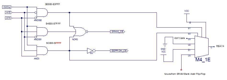
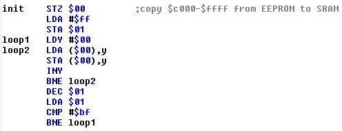
Copy software, pretty simple, it stays within boundaries. It should take about 2-3 sec? to complete @2.5Mhz:
Edit: added software pic & 4bit counter is upper left (correction), not upper right.
Last edited by ElEctric_EyE on Tue Aug 24, 2010 2:08 am, edited 3 times in total.
Hmmm. "O2OUT" is Phase Two? If so, it looks to me as if the RBA14 signal (SRAM bank addr) can change state when phase 2 goes true. That ought not to be the case; address lines on the SRAM should already be stable by the start of phase 2 (ie, when CS activates). This might not be what's causing your difficulty, though.
Garth's suspicion about bus contention rings true... FWIW, my oscilloscope suggestion can reveal stuff like that, whether due to wiring errors or design issues. But I haven't described it in proper detail I'm afraid.
-- Jeff
Garth's suspicion about bus contention rings true... FWIW, my oscilloscope suggestion can reveal stuff like that, whether due to wiring errors or design issues. But I haven't described it in proper detail I'm afraid.
-- Jeff
Last edited by Dr Jefyll on Thu Aug 12, 2010 5:42 am, edited 1 time in total.
-
ElEctric_EyE
- Posts: 3260
- Joined: 02 Mar 2009
- Location: OH, USA
Dr Jefyll wrote:
Hmmm. "O2OUT" is Phase Two? If so, it looks to me as if the RBA14 signal (SRAM bank addr) can change state when phase 2 goes true. That ought not to be the case; address lines on the SRAM should already be stable by the start of phase 2 (ie, when CS activates). This might not be what's causing your difficulty, though...
The only I/O device I have at this point is the display @$8000,$8001. As an experiment I took phase 2 out of the decoding for it, and it was receiving data, erroneously, but the display was changing.
I'm pretty sure everything is wired correctly, I've doube, triple checked my wiring, rechecked the QFP to BGA adapter pinouts, and ohmed out a few pins direct from each of the IC's (54-pin TSOPII SRAM & 100-pin VQFP FPGA) to the wirewrap pins. To make sure my soldering is 100%, I guess I should check all pins, but before I spent that much time...
So the idea of "Locking" 16K blocks, which is really bank switching, is not a problem? Even in the middle of a program?