6502.org Forum  Projects  Code  Documents  Tools  Forum
It is currently Sat Apr 27, 2024 8:10 pm

All times are UTC


Post new topic Reply to topic  [ 56 posts ]  Go to page Previous  1, 2, 3, 4  Next
Author Message
PostPosted: Thu Dec 16, 2021 9:46 am 
Offline
User avatar

Joined: Wed Feb 14, 2018 2:33 pm
Posts: 1399
Location: Scotland
AndrewP wrote:
drogon wrote:
The obvious missing things might be network and a web browser. A modern web browser is an operating system in itself now.
Agreed. I have complaint about how browsers are so complicated that they basically prevent any new competition.


Not just browsers, but general graphical components too - posting this here as it's relevant to multi-threading/multi-processing which is a goal:

https://www.da.vidbuchanan.co.uk/widgets/pngdiff/

-Gordon

_________________
--
Gordon Henderson.
See my Ruby 6502 and 65816 SBC projects here: https://projects.drogon.net/ruby/


Top
 Profile  
Reply with quote  
PostPosted: Sat Dec 18, 2021 7:55 am 
Offline
User avatar

Joined: Mon Aug 30, 2021 11:52 am
Posts: 251
Location: South Africa
BigEd wrote:
Although this isn't quite the thread title for this discussion, now I look at it, your new thread didn't feel like quite the right one for these comments of mine. As they say, Naming Things is one of the hard problems of computer science. In this case, naming threads.

Your answer to
- what should this system be able to do
is probably something like
- get useful work out of multiple CPUs simultaneously
and your preferred tactic - your proposed organisation - is to use shared memory, but memory that's significantly faster than the CPUs.

Once you can set down these kinds of statements about your project, you can avoid the side-discussions about other goals and other ways of achieving your goal.
Thanks, these are really good suggestions. Also somewhere you mentioned block diagrams and I'm coming to realise how important these are. Not just for myself (I have one kinda scribbled down and keep the context in my head) but for everyone else here. It can't be fun spending the time trying to work out what someone is doing at a high-level from schematic, that's a significant mental undertaking.

GARTHWILSON wrote:
Andrew, I think this topic and the links in it will be of interest, regarding multiprocessing:
Theoretical question - Multiple CPU's
Thanks! That's some good reading in there. A rabbit hole of links to links to links :D


Top
 Profile  
Reply with quote  
PostPosted: Sat Dec 18, 2021 8:03 am 
Offline
User avatar

Joined: Mon Aug 30, 2021 11:52 am
Posts: 251
Location: South Africa
Dr Jefyll wrote:
Image
Thanks! That's most helpful. I'll post up yet another thread on detecting interrupts before the stack manipulation takes place a bit later. But... there was an incident. I'd mostly simulated up your schematic in Logisim when my dog - who was sleeping under the desk - woke up, banged his head on a drawer, panicked and then proceeded to flip the desk over. Destroying my monitor in the process. It's a bit annoying that I have to replace my monitor but more annoying that I hadn't saved my Logisim project and shutdown everything before I realised. Doh.

When I have the energy I'll redo the simulation to make sure I understand what's happening.

ps: That's a nice usage of a '238 there. I would never have thought of that.


Top
 Profile  
Reply with quote  
PostPosted: Sat Dec 18, 2021 1:19 pm 
Offline
User avatar

Joined: Fri Dec 11, 2009 3:50 pm
Posts: 3346
Location: Ontario, Canada
Quote:
Destroying my monitor in the process.
Oh, dear! So now the monitor becomes a prospective organ donor! :| (But hopefully not the dog!) :wink:

_________________
In 1988 my 65C02 got six new registers and 44 new full-speed instructions!
https://laughtonelectronics.com/Arcana/ ... mmary.html


Top
 Profile  
Reply with quote  
PostPosted: Tue Dec 21, 2021 7:27 am 
Offline
User avatar

Joined: Mon Aug 30, 2021 11:52 am
Posts: 251
Location: South Africa
Dr Jefyll wrote:
Quote:
Destroying my monitor in the process.
Oh, dear! So now the monitor becomes a prospective organ donor! :| (But hopefully not the dog!) :wink:
Attachment:
20211219_073006.jpg
20211219_073006.jpg [ 662.96 KiB | Viewed 7769 times ]
A pot plant went through the panel but fortunately I have a second identical monitor with a dodgy control board* so now I have one working monitor.

Poor gooey old dog is fine although he had a bit to say about the desk attacking him and then demanded treats. :lol:

*It failed two weeks after warranty and Dell were, like, "Nope, buy a new one".


Top
 Profile  
Reply with quote  
PostPosted: Sat Dec 25, 2021 12:34 pm 
Offline
User avatar

Joined: Mon Aug 30, 2021 11:52 am
Posts: 251
Location: South Africa
Another quick update. I've added a few more ICs into the simulation. Specifically the '157, '574 and the '0102.

Attachment:
StableV1.1.png
StableV1.1.png [ 16.85 KiB | Viewed 7725 times ]


The news I meant to mention earlier was that whilst my pull request was accepted into the release candidate for Logisim Evolution 3.7.2 the file it was in was then reverted. I'll need to submit another pull request to try and get it into 3.7.3 but that means I still can't do a public release yet.

ps:
Dr Jefyll wrote:
Variations are possible, of course, but this explains how hardware interrupts can be detected prior to the vector fetch. It also explains how execution of any specific opcode can be detected.
I still haven't gotten around to re-simulating the circuit you posted but I will eventually get there and post it into it's own interrupt detection thread.


Top
 Profile  
Reply with quote  
PostPosted: Fri Mar 11, 2022 4:26 pm 
Offline
User avatar

Joined: Mon Aug 30, 2021 11:52 am
Posts: 251
Location: South Africa
This is kind of a sad post for the Logisim Project. I've pushed Logisim Evolution beyond what it was intended for and it has gotten to the point where I'm spending more time working around simulation issues than doing design work. I think it's truly amazing what can be achieved in it and it's given me a lot of insight into just how complicated building logic out of discrete circuits is. Ultimately though I've had to end the project because it's too slow, too limited and - as I'm working in my own fork - unusable by anyone else.

My end goal was was to simulate a 'modern' home computer made entirely from discrete ICs with the intent of having something that can be fully understood, built and used by a hobbyist. (It's turned out to be WAY more complex than I thought but still mostly within the realm of reason).

This post isn't just to announce the end of the Logisim Project but also just to give a bit of a view into what I had managed to achieve.

Attachment:
HCP65.png
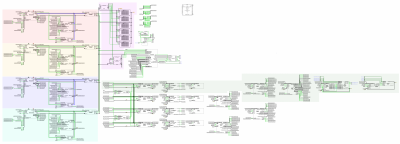
HCP65.png [ 616.42 KiB | Viewed 7515 times ]
Above is the high level 'motherboard' circuit (somewhat akin to the block diagram BigEd suggested I post ages ago and which I really will... one day).

There are four '816 processes each running with their own private RAM in the four similarly shaped and coloured blocks on the left hand side. There are also four graphics blitters (basically memory copiers) that run in the same memory 'channel' as the MPU in the block with it.

Main memory in the purple block in the top middle can be accessed in time based 'channels'*. The first '816 or blitter gets 25ns of RAM access time then the second '816 gets 25ns of access time then the third and fourth. For a total of four distinct accesses across 100ns. Each '816 runs at 10MHz and each PHI2 clock signal is offset is by 25ns from the previous.

If the '816 is running in private memory then the blitter on the same channel is free to copy bytes (a single row of pixels in a sprite for example) from main memory into video memory. The blitters understand transparency and are mostly intended for drawing graphics but can be used to copy any block of memory from main or video memory to main or video memory. Each blitter is also run on the same 10MHz clock as the '816 on the same channel and takes 3 cycles to draw 2 pixel. One blitter just isn't enough for decent framerates, that's why there are four :mrgreen:

The video board is a pair of flipping frame buffers. It's by far the most complicated circuit I've ever designed but not very interesting in terms of what it does; it's just a palettised RAMDAC.

The devices are each 16 bytes of addressable memory somewhere in the zero'th bank. Any '816 can access any device (although they need to negotiate single access amongst themselves first). I've had to do a bit of clock stretching for device reads as there is no way at all a device could respond within 25ns; I've quartered the clock speed to give a device closer to 350ns to respond. Writes are not clock stretched.

This is a very high level summary of what's been simulated in Logisim and each of the 'components' on the 'motherboard' works in simulation. Unfortunately running whole motherboard immediately starts oscillating so I've never seen the computer actually run.

Moving on and drilling down into one of the Microprocessor sub-circuits as an example.
Attachment:
MPU Kernal Only.png
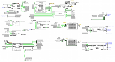
MPU Kernal Only.png [ 128.86 KiB | Viewed 7515 times ]
This one is probably pretty self-explanatory as it's similar to (and inspired by) lots of previous W65C816 builds.

On this board is an actual microprocessor and 128KB of SRAM that the '816 runs in when in the first 128K addresses.

Clock control is responsible for the mentioned clock stretching, down to 2.5MHz for devices and 5MHz for ROM access. Interrupt Vectoring does what it says on the tin. The Flags register contains a latch that holds two bits of information. The first is whether or not the ROM is addressable; the idea being the ROM is copied into RAM and then turned off. The second is 'lock-in' mode, the clock is increased to 20MHz but all address decoding is disabled allow only the 128K of private memory to be accessed.

The Selector State takes the incoming clock signals and enables or disables various components on the board based on time into PHI2. The Memory Transceiver allows the address and data busses out to the main memory seen on the 'motherboard' and the Device Gateway does the same for devices.

Address Decode also does what it says on the tin but it's composed of the most discrete ICs out of any of the sub-circuits on this board. And as someone asked: "How much decoding is too much address decoding" I think I can answer that :shock:
Attachment:
Address Decode.png
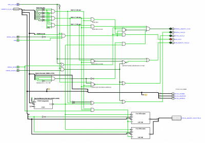
Address Decode.png [ 64.24 KiB | Viewed 7515 times ]
I'm not going to describe it - there's been enough of that in this post already. I'm just using it as an example of what I did manage in Logisim now that we've finally drilled down to a sub-circuit that's composed only of discrete components.

So that's it. I've learned a lot on my Logisim journey. I like to think I've achieved quite a lot too but that isn't very useful to anyone else in the community :?

However I'm a crazy bastard and so whilst the Logisim Project is ended the journey doesn't stop here! Soon** there will be a better more stable simulator but that's a post for another time.

* I need a better word than channel but I can't think of anything.
** Soon may be subject to unforeseen temporal fluctuations.


Top
 Profile  
Reply with quote  
PostPosted: Fri Mar 11, 2022 4:50 pm 
Offline
User avatar

Joined: Thu Dec 11, 2008 1:28 pm
Posts: 10793
Location: England
Thanks for writing up where you'd got to - that's much preferable to a silence from an abandoned project. And good to hear that you've learned a lot. Hopefully that will feed in to a subsequent project.


Top
 Profile  
Reply with quote  
PostPosted: Sun Mar 20, 2022 2:49 pm 
Offline
User avatar

Joined: Mon Aug 30, 2021 11:52 am
Posts: 251
Location: South Africa
BigEd wrote:
Thanks for writing up where you'd got to - that's much preferable to a silence from an abandoned project. And good to hear that you've learned a lot. Hopefully that will feed in to a subsequent project.
No prob! And my old Logisim project is already feeding pretty directly into the new project 8)

It's not deserving of a new thread yet but what I've managed to do is to entirely parse my Logisim circuit files into a C++ based simulator project. A small step, but a useful one.


Top
 Profile  
Reply with quote  
PostPosted: Tue Mar 22, 2022 12:13 pm 
Offline
User avatar

Joined: Tue Aug 11, 2020 3:45 am
Posts: 311
Location: A magnetic field
AndrewP on Fri 11 Mar 2022 wrote:
The second is 'lock-in' mode, the clock is increased to 20MHz but all address decoding is disabled allow only the 128K of private memory to be accessed.


I've doodled multi-core designs and found that it is possible to have eight cores on one clock phase and eight cores on the opposite clock phase. Unfortunately, the whole cluster is paused when any core made a slow access - and this becomes increasingly likely when there are more cores. However, it never occurred to me that any core may provide an explicit hint and opt-out of clock stretching. There might be an edge case where a core re-joins at the end of a long clock stretch. Regardless, the principle and the efficiency is fantastic.

After your experiments with logic simulation, you may have further insights. I am amazed that FPGA and similar are so astounding bad when implementing a bus structure. It is a very common requirement. For example, when implementing peripheral registers. Arbitrary bus driving may be an awkward case but even in the trivial case, a tri-state return path can be difficult or impossible. I believe you also had difficulty implementing MCP101/DS1813 reset functionality.

Beyond tri-state logic and an explicit time-step for simulation, what else is commonly broken and how would you implement it?

_________________
Modules | Processors | Boards | Boxes | Beep, Beep! I'm a sheep!


Top
 Profile  
Reply with quote  
PostPosted: Thu Mar 24, 2022 11:39 am 
Offline
User avatar

Joined: Mon Aug 30, 2021 11:52 am
Posts: 251
Location: South Africa
Sheep64 wrote:
I've doodled multi-core designs and found that it is possible to have eight cores on one clock phase and eight cores on the opposite clock phase. Unfortunately, the whole cluster is paused when any core made a slow access - and this becomes increasingly likely when there are more cores. However, it never occurred to me that any core may provide an explicit hint and opt-out of clock stretching. There might be an edge case where a core re-joins at the end of a long clock stretch. Regardless, the principle and the efficiency is fantastic.
Thanks!

Yup, the rejoin is unpleasant.
Attachment:
PHI2 Timing.png
PHI2 Timing.png [ 62.95 KiB | Viewed 7369 times ]
I generate my clock signal as in the piccy above. In 10Mhz mode ('normal access mode') the write is always held until the end of PHI2 (specifically it is held until SEL6) so the latch that determines if it is in 20Mhz ('lock-in mode') is written late enough that PHI2 stays high.

The problem is when the latch is written in 'lock-in' mode during the first short PHI2 cycle (i.e written during SEL4). Addressing is reenabled but some addressing operations that should have happened in SEL2 and SEL3 when in normal access mode have not have happened. And so who knows what the poor '816 will actually address in the end. It is in a horribly inconsistent state.

To fix this I have a flip-flop behind the latch that controls lock-in. Even if a write to that latch is done during SEL4 the flip-flop only updates on SEL6 and so (hopefully) consistency is preserved. This is all still in simulations so I don't know if it will work in the real world.

In your 16 core model do you have all the '816s addressing separate SRAM ICs? I can't get more than 4 addressing a single shared memory. Even using 10ns SRAM the fastest I can read from it is in 25ns. That means that each '816 has to be in and out within 25ns or it steps on the next one's toes. (25ns *4 = 100ns is where the maximum 10Mhz I can run at when accessing main memory comes from).

Sheep64 wrote:
Beyond tri-state logic and an explicit time-step for simulation, what else is commonly broken and how would you implement it?
Another post incoming because that has a long answer. :D


Top
 Profile  
Reply with quote  
PostPosted: Sun Mar 27, 2022 4:50 pm 
Offline
User avatar

Joined: Mon Aug 30, 2021 11:52 am
Posts: 251
Location: South Africa
Just a quick message because it's been ... one of those weekends.

I finally got something specific-to-computer-hardware-building going. Wheee!

Best yet it's based off of the Logisim simulation I did and it actually seems to work. At it's heart it's pretty simple idea. Shift in 12 bits from a SNES controller and shift them out into a register. The two boards you see generate the latch and clock signals to the SNES controller; and the shift clock to a pair of '595 shift registers (shown further down).
Attachment:
SNES Signal Generator.jpg
SNES Signal Generator.jpg [ 1.66 MiB | Viewed 7329 times ]
Of course nothing is every simple and the '373 latch I hide all the combinatorial logic behind is the wrong size for the footprint I used. The values that would be latched (had there been, you know, a latch) look right but now I'm stuck waiting for a smaller '373 to arrive.

The schematic below is for the board on the left (you can see the little clock oscillator on it). The controller_clock and controller_latch are the signals that go to the SNES controller (after some voltage translation). Shift_in_clock goes to the pair of '595 shift registers.
Attachment:
SNES Counter Schematic.png
SNES Counter Schematic.png [ 9.69 KiB | Viewed 7329 times ]

(Again) the schematic below is the combinatorial logic to ensure I get a decently long latch signal (the SNES shift register is not a fast IC at 5V) and also 12 nice long clock signals. /Done_shifting stops the process until the controller needs to be read again.
Attachment:
SNES Timing Schematic.png
SNES Timing Schematic.png [ 9.55 KiB | Viewed 7329 times ]

On the other side are the shift registers (two per controller for 8 in total). This is what is meant by a multi-layer board right? And the device address selector (top right) to allow the '816 to talk to those registers as well as the voltage translation (at the bottom plugged into the SNES ports).
Attachment:
SNES Latch Device.jpg
SNES Latch Device.jpg [ 1.48 MiB | Viewed 7329 times ]

Not much more to say here. Just excited to finally have something non-simulation to show :)

And, Sheep, this does kinda lead into your question because it was such a mission going from Logisim to physical PCB. I will - eventually - type up my answer on what I think needs to be fixed and improved in Logisim.

I forgot to mention: the big board at the back just reads signals and gives me up to 5 bytes of hexadecimal display for those signals. It's a horrible implementation and I really need to redesign it but for now it just barely scrapes along and allows me to see whats on a bus etc...


Top
 Profile  
Reply with quote  
PostPosted: Thu Mar 31, 2022 6:37 pm 
Offline
User avatar

Joined: Mon Aug 30, 2021 11:52 am
Posts: 251
Location: South Africa
Sheep64 wrote:
Beyond [bi-directional ports] and an explicit time-step for simulation, what else is commonly broken and how would you implement it?
I wouldn't say much is explicitly broken in Logisim (except saving large files and propagations in large circuits). Rrather there are requirements I have of Logisim that it was never designed for.

With that said my first change would be bidirectional ports - clearly a Logisim deficiency. Ports between sub-ciruits are either inputs or outputs and that's a huge problem for the data bus. So:

1) Bidirectional ports

2) Time based simulation, more specifically events that take time to propagate. This is both for more accurate simulation and to stop simulation oscillations.

3) Performance. Logisim is slow. My simulated computer struggles to crack 19Hz when running the entire simulation on a i9 9900K.

4) Test cases. I need some way to define unit tests. I occasionally I break a wire or bump a gate and it can take ages to notice. (Incidentally Digital has units tests and is much faster Logisim)

5) A bunch of quality of life fixes. Things like the ability to highlight multiple nets and refactor tunnel names etc..

And that's kind of it for a logic simulator. Logisim but betterer.

But things don't end there and now I start touching on my previous post. I'm not just interested in the logic simulation side of things; I want a physical board at the end of this. I use KiCad (another amazing free program) and to a large extent there's a one-to-one match between my Logisim circuit and my KiCad schematic. Drawing those schematics is tedious and I make mistakes. I don't like either of those. It would be easier if I could export my simulation out to a KiCad schematic file. It would be hard, but not impossible, to use KiCads symbols in my own simulator editor to make this export process practically transparent.

I have a lot of circuits in my simulation. It takes me about a week to transcribe just one. If I can automate this I may even end up saving myself time in the long run. Doubtful. But maybe.

That includes routing PCBs. KiCad used to have a (poor) auto-router but it's since been removed and the new one has not yet been added. I have a fairly specific set of requirements so writing my own component placer / auto-router is not quite as mad as it sounds. I don't have to provide a general solution and I have PCB constraints that I can infer or define at the simulation level. I also have a bit of experience programmatically placing and packing connected objects with physical constraints. Not so different from placing and routing components on a PCB.

Ultimately what I need is a logic simulator that is voltage and IC aware without being a full electronic simulator. I need it to be easy to use and fast as well as having the ability to export to KiCad. A big ask but hopefully worth it in the end.


Top
 Profile  
Reply with quote  
PostPosted: Sat Apr 02, 2022 1:05 pm 
Offline
User avatar

Joined: Sat Jul 24, 2021 1:37 pm
Posts: 282
Have you tried Digital? https://github.com/hneemann/Digital

_________________
BB816 Computer YouTube series


Top
 Profile  
Reply with quote  
PostPosted: Mon Apr 04, 2022 9:23 am 
Offline
User avatar

Joined: Mon Aug 30, 2021 11:52 am
Posts: 251
Location: South Africa
akohlbecker wrote:
Have you tried Digital? https://github.com/hneemann/Digital
I did, thanks. And generally Digital seems a lot more modern than Logisim. The problem I ran into was that I could find no documentation or examples on how to implement my own ICs in Digital.

As an aside I should mention I'm (still) really enjoying your YouTube series. I also like your 8-bit hex display thing, it seems really useful.


Top
 Profile  
Reply with quote  
Display posts from previous:  Sort by  
Post new topic Reply to topic  [ 56 posts ]  Go to page Previous  1, 2, 3, 4  Next

All times are UTC


Who is online

Users browsing this forum: No registered users and 6 guests


You cannot post new topics in this forum
You cannot reply to topics in this forum
You cannot edit your posts in this forum
You cannot delete your posts in this forum
You cannot post attachments in this forum

Search for:
Jump to: