6502.org Forum  Projects  Code  Documents  Tools  Forum
It is currently Sat Apr 27, 2024 5:36 pm

All times are UTC


Post new topic Reply to topic  [ 164 posts ]  Go to page Previous  1 ... 7, 8, 9, 10, 11  Next
Author Message
PostPosted: Wed Sep 14, 2016 11:56 am 
Offline
User avatar

Joined: Fri Nov 09, 2012 5:54 pm
Posts: 1392
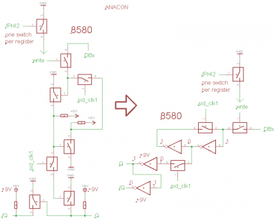
Now about the switches.

From the logic design point of view, the registers which control all the switches
and the filter frequency DAC all have identical schematics.

The layout for the register bits varies a little to make better use of the space
on the silicon, also size\geometry of the FET at the output might vary a little
depending on the load it has to drive...

Schematic for one register bit:

Attachment:
8580_anacon.png
8580_anacon.png [ 15.55 KiB | Viewed 11059 times ]


BTW: the PolySi write control lines are a bit long, so the designers added a FET to every 8 bit register
as a "kludge" to meet the bus hold timing that clobbers the write control signal to GND if PHI2 =0...
like with the registers in the envelope generator.

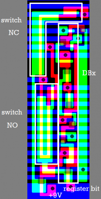
The game is similar like in the 6581... except for one thing:
each of the switches is built from two FETs instead of just one FET.

Attachment:
s8580_anacon.png
s8580_anacon.png [ 14.05 KiB | Viewed 11059 times ]


East, we have a big PolySi pad that connects to a bit on the internal data bus.

West, we have two analog switches,
one normally open (NO) // closed, if the register bit is written with 1
one normally closed (NC) // closed, if the register is written with 0
BTW: geometry\ratio of the FET that works as an analog switch gives the resistance of a closed switch.

...and in the middle, we have the register bit.

;---

In the 6581, we had one FET working as a switch for an analog signal.

In the 8580, we have _two_ FETs working as a single switch for an analog signal:
A FET with a low impedance and a FET with a high impedance in series.
IMHO this might be a trick from the designers to reduce capacitance between both ends of a switch.
The FET with the higher impedance tends to be at the side of the switch that connects to an OP or such...

Note, that this trick is also used in the frequency control DACs...
and maybe for resistors which don't act as a switch, too.


Top
 Profile  
Reply with quote  
PostPosted: Wed Sep 14, 2016 12:17 pm 
Offline
User avatar

Joined: Fri Nov 09, 2012 5:54 pm
Posts: 1392
The 4.759V voltage for the virtual ground is generated by a PolySi resistor divider
north east from the LSB of the channel 3 envelope DAC.

Attachment:
s8580_ref.png
s8580_ref.png [ 10.48 KiB | Viewed 11059 times ]


Attachment:
8580_ref.png
8580_ref.png [ 19.76 KiB | Viewed 11059 times ]


...we'll see about that OpAmp later.


Top
 Profile  
Reply with quote  
PostPosted: Wed Sep 14, 2016 12:42 pm 
Offline
User avatar

Joined: Fri Nov 09, 2012 5:54 pm
Posts: 1392
Unlike the 6581, the 8580 has real OpAmps:

Attachment:
s8580_opamp.png
s8580_opamp.png [ 38.54 KiB | Viewed 11058 times ]


Attachment:
8580_opamp.png
8580_opamp.png [ 26.14 KiB | Viewed 11058 times ]


// sorry for the size of those pictures.

In the differential amplifier sensing +in and -in, we have 4 FETs instead of two.
That's a temperature compensation.

I remember from my transistor OpAmp experiments, that when just touching
one of the two transistors in the differential input amplifier with my finger,
this caused the output of my OpAmp to go off by 10V or such just because
of the temperature difference between those two transistors...

But back on topic:
The output buffer circuitry looks a bit complicated, the constant current sink in the differential
input amplifier looks complicated, too. If you want to know how it works in detail,
you better consult an engineer. :)

Layout for all the OpAmps in the 8580 looks pretty much similar,
except that the OpAmp which generates the gate voltage for the frequency control DACs
has a smaller feedback capacitor... in other words, it's supposed to be faster than the others.


Top
 Profile  
Reply with quote  
PostPosted: Wed Sep 14, 2016 1:28 pm 
Offline
User avatar

Joined: Fri Nov 09, 2012 5:54 pm
Posts: 1392
At some point, I noticed two big capacitors in the 8580 layout.

So I started to wonder, what they might be good for.

Voltage doubler charge pump ? Can't be, because all the OpAmps turned out to be +9V powered.
Switched capacitor filter ? Can't be, because of how the switches attached to those capacitors are wired up.

It turned out that the two big capacitors are part of a trick circuitry,
which changes the gate voltage of the frequency control DACs according
to the temperature of the DACs, to reduce the effects of temperature
to the filter curve.

There is a FET working as a temperature sensor close to the DACs...
but we are getting there later.

Attachment:
8580_cap.png
8580_cap.png [ 116.53 KiB | Viewed 11055 times ]


We have an asynchronous 3 bit binary counter, LSB is running at the speed of PHI2.
Every counter bit drives a R\S flipflop for making the inverted and non_inverted
output of the bit non_overlapping.

From the logic design point of view, those three bits in the counter are pretty similar...
on the silicon, the transistors in the R\S flipflop output of the MSB are just a bit bigger...
and +9V powered.

Attachment:
s8580_capcnt.png
s8580_capcnt.png [ 33.79 KiB | Viewed 11055 times ]


The two big capacitors and the +9V powered switches "between" them:

Attachment:
s8580_capsw.png
s8580_capsw.png [ 29.24 KiB | Viewed 11055 times ]


It's an ingenious idea to use the AC resistance of two capacitors as a voltage divider.

The AC resistance of the two capacitors depends on the PHI2 clock frequency,
while the resistance of the temperature sensor FET does not.

This implicates, that when taking a PAL C64 and modiying it into a NTSC C64,
or vice versa, this might shift the filter curve by 4% or such.


Top
 Profile  
Reply with quote  
PostPosted: Wed Sep 14, 2016 3:33 pm 
Offline
User avatar

Joined: Fri Nov 09, 2012 5:54 pm
Posts: 1392
Schematic for a register bit plus frequency control DAC buffer:

Attachment:
8580_freqdacbuf.png
8580_freqdacbuf.png [ 17.75 KiB | Viewed 11046 times ]


Nothing special, conceptually the DAC buffer is just a super buffer... but it's +9V powered.
The output either is tied to GND, or to the gate control voltage mentioned in the previous post.

We have two identical 12 bit DACs in the 8580, which work as resistances for the filter integrators:

Attachment:
s8580_freqdac.png
s8580_freqdac.png [ 142.49 KiB | Viewed 11046 times ]

// sorry for those colors.

The 8580 has 11 bits for frequency control, but 12 bit DACs.
If those 11 bits would be '0', the impedance of the DACs would be "infinitely high".
To get around this, there is an 11 input NOR gate below the DACs sensing those 11 bits.
If they are 0, the NOR gate gives the gate control voltage to the 12 bit DAC LSB.

Between the DACs and the NOR gate, we have that FET which works as a temperature sensor
for the circuitry that changes the gate control voltage according to the DAC temperature.

Schematic for one of the two DACs:

Attachment:
8580_freqdac.png
8580_freqdac.png [ 18.47 KiB | Viewed 11046 times ]


Like with the other analog switches in the 8580,
in the DAC we have _two_ FETs working as a single switch for an analog signal:
A FET with a low impedance and a FET with a high impedance in series.
IMHO this might be a trick from the designers to reduce capacitance between both ends of a switch.
The FET with the higher impedance tends to be at the side of the switch that connects to an OP or such...


Top
 Profile  
Reply with quote  
PostPosted: Wed Sep 14, 2016 3:46 pm 
Offline
User avatar

Joined: Fri Nov 09, 2012 5:54 pm
Posts: 1392
Ah, I nearly forgot:

For resonance control, we have two more tiny DACs and a little bit of decoding for them.
That stuff is located north of the "BP feedback" OpAmp on the silicon.

Attachment:
s8580_reso.png
s8580_reso.png [ 46.21 KiB | Viewed 11046 times ]


Schematic:

Attachment:
8580_reso.png
8580_reso.png [ 70.58 KiB | Viewed 11046 times ]


'Gate_RR0'..'Gate_RR7' in the schematic above is just the gate voltage for the analog resonance switches R0..R7.
Again two FETs of different resistance in series for every switch,
and the geometry\ratio of the FETs defines the switch resistance when the switch is closed.

Nothing fancy in there...


Top
 Profile  
Reply with quote  
PostPosted: Wed Sep 14, 2016 3:54 pm 
Offline
User avatar

Joined: Fri Nov 09, 2012 5:54 pm
Posts: 1392
Ok, now for my interpretation of the 8580 filter:

Attachment:
8580_filter.png
8580_filter.png [ 152.62 KiB | Viewed 11047 times ]


There is a nice picture of the 8580 filter section at Tommi Lempinen's site,
but the picture is a little bit too big for directly linking to that image...
and making the image smaller would spoil the readability of it:
http://oms.wmhost.com/misc/MOS_8580_R5_filter.png


Top
 Profile  
Reply with quote  
PostPosted: Wed Sep 14, 2016 4:01 pm 
Offline
User avatar

Joined: Fri Nov 09, 2012 5:54 pm
Posts: 1392
Just adding a few little AppNotes related to calculating/building filters for those who might be interested...

...and with that, I'm through. Woot.

Can't believe that I got all that stuff off my desk.

Now to send my brain on vacation...
...hoping that drfiemost will fill some of the potholes in my postings. :)

Edit:
Designing Analog Chips by Hans Camenzind (inventor of the NE555).
Now that's an interesting read: some basics about transistors, OpAmps, filters, DACs...


Attachments:
tidu543.pdf [2.02 MiB]
Downloaded 273 times
MT-223.pdf [82.63 KiB]
Downloaded 246 times
MT-208.pdf [160.49 KiB]
Downloaded 241 times
MT-205.pdf [86.38 KiB]
Downloaded 246 times
sbfa005.pdf [32.2 KiB]
Downloaded 247 times


Last edited by ttlworks on Sat Jan 12, 2019 3:10 pm, edited 1 time in total.
Top
 Profile  
Reply with quote  
PostPosted: Thu Sep 15, 2016 5:17 am 
Offline
User avatar

Joined: Fri Nov 09, 2012 5:54 pm
Posts: 1392
Eagle 6.4 schematics, source for my schematics pictures in this thread.
For those who want to correct errors, or who want to modify/customize them for writing articles.

'Free' as in 'free beer', all rights reversed, etc.
Might require some work, have fun.


Attachments:
sid.zip [566.04 KiB]
Downloaded 266 times
Top
 Profile  
Reply with quote  
PostPosted: Sun Sep 18, 2016 9:54 pm 
Offline

Joined: Sun Sep 18, 2016 9:33 pm
Posts: 3
ttlworks wrote:
At some point, me and drfiemost had started to wonder how much time and effort
went into generating those vectorized polygon pictures.

It's a manually routed chip layout, silicon might have some impurities,
so automated tools for processing the silicon picture probably won't bring you far.

Just trying to figure out what the diffusion layer might look like for one of the
sprite X\Y registers in a VIC2 took me a full day. :)
Considering this, only having four bugs in the polygon pictures of the SID
is very impressive !

;---

With our little SID dissection here in the forum, we are standing on the shoulders
of those who de_capped the chips, made the high resolution silicon pictures,
and generated the vectorized polygon pictures.


Without this work being done before, we would have had as much chance as a snowball in hell...


Thank you guys for going another insane route and further documenting the inner workings of the SID! :D

Michael Huth from Max Planck Institute is who took the original photos of the chips I had decapped (without acids, just by brute force method), and tiled the full images after which I started working on the filter section just by curiosity, and eventually ended up redrawing the complete chip.

Was expecting there to be some errors. The repeated error on all three channels is due to copying over sections from one channel to another after having finished one channel. Also with the 8580 there are sections I still do not fully understand...

Started with the 6581R3 early 2008 and it took about two months to "complete" the image. Having very little understanding about chip construction before I had to read about chip design a little bit to understand some what I was looking at. R2 and R4 came afterwards, but was much quicker after just comparing what's different between the revisions. 8580 again took about two months as it was almost completely redrawn from scratch.

Tommi Lempinen


Top
 Profile  
Reply with quote  
PostPosted: Mon Sep 19, 2016 3:21 am 
Offline
User avatar

Joined: Thu Dec 11, 2008 1:28 pm
Posts: 10793
Location: England
Thanks for dropping by, Tommi, and thanks for all the work you put in!


Top
 Profile  
Reply with quote  
PostPosted: Tue Sep 20, 2016 7:07 pm 
Offline

Joined: Sun Sep 18, 2016 9:33 pm
Posts: 3
Would be very interesting so see if anyone could recreate the SID the hard way without resorting to programmable logic. Tho I've been asked many times if it could be remanufactured from the images, and once even offered the costly possibility of attempting to do so.

I'm into all this rather from the point of preservation, be is soft- or hardware. :)


Top
 Profile  
Reply with quote  
PostPosted: Tue Sep 20, 2016 7:13 pm 
Offline
User avatar

Joined: Thu Dec 11, 2008 1:28 pm
Posts: 10793
Location: England
Well, the MonSter6502 was very impressive, but not real-time, and one thing you'd need with a SID recreation would be realtime and analogue fidelity. That's a tall order! Even if you could fund a real fabricated chip, you'd need lots of care to get the parasitic and transistor behaviours right. And if the chip doesn't work, as they very often don't, you need the funds to go around a second time.

Perhaps you could recruit a student in a fancy university who will get a chip made as a term project?


Top
 Profile  
Reply with quote  
PostPosted: Wed Sep 21, 2016 6:12 am 
Offline
User avatar

Joined: Fri Nov 09, 2012 5:54 pm
Posts: 1392
One problems is, that manufacturing chip prototypes won't be cheap, even as a university project.

Another problem is, that the manufacuring process available probably would aim for something
like less than 1 micrometer 3.3V CMOS...
while 8580 was 2 micrometers NMOS, and partially +9V powered.

This asks for a complete redesign of the analog part, especially the filter section.

Also, we could expect to have some difficulties when it comes to mixing waveforms,
2 micrometer 8580 already sounded a bit different than 7 micrometer 6581,
although the layout for the waveform selector switches looks somewhat similar
for both chips.

;---

Would say, that some more research has to be done by interpreting the results of our SID dissection,
and before trying to build a chip I'd highly recommend to build a prototype from standard parts
"out of the drawer" and without resorting to programmable logic.

Unfortunately, I'm not longer active...
But if we just wait a few more years, maybe somebody else will make a try. :)


Top
 Profile  
Reply with quote  
PostPosted: Wed Sep 21, 2016 2:55 pm 
Offline
User avatar

Joined: Fri Nov 09, 2012 5:54 pm
Posts: 1392
@ BigEd:
I'm somewhat hesitant to ask this, but...

Any chance to find out what the transfer curves (gate voltage versus drain\source resistance) for NFETs
manufactured in a 7 micrometer NMOS process and in a 2 micrometer HMOS-2 process may look like ?


Top
 Profile  
Reply with quote  
Display posts from previous:  Sort by  
Post new topic Reply to topic  [ 164 posts ]  Go to page Previous  1 ... 7, 8, 9, 10, 11  Next

All times are UTC


Who is online

Users browsing this forum: No registered users and 9 guests


You cannot post new topics in this forum
You cannot reply to topics in this forum
You cannot edit your posts in this forum
You cannot delete your posts in this forum
You cannot post attachments in this forum

Search for:
Jump to: