6502.org Forum  Projects  Code  Documents  Tools  Forum
It is currently Sun Apr 28, 2024 8:04 am

All times are UTC


Post new topic Reply to topic  [ 164 posts ]  Go to page Previous  1 ... 6, 7, 8, 9, 10, 11  Next
Author Message
PostPosted: Tue Sep 13, 2016 6:10 am 
Offline
User avatar

Joined: Fri Nov 09, 2012 5:54 pm
Posts: 1392
List of the bugs in the vectorized polygon pictures we found so far,
and their X/Y coordinates in the picture.

Orientation: filter section is south.

;---

MOS_6581R2_full.png //date: 01 Aug 2010 //size: 16820*14629

Missing via for PWM upper register write: 4780/5133, 9031/5133, 13280/5133
Missing GND connection for paddle counter LSB carry input: 6935/12953

;---

MOS_6581R3_full.png //date: 01 Aug 2010 //size: 16820*14629

Missing via for PWM upper register write: 4780/5133, 9031/5133, 13280/5133
Missing GND connection for paddle counter LSB carry input: 6940/12953

;---

MOS_6581R4_full.png //date: 01 Aug 2010 //size: 16820*14629

Missing via for PWM upper register write: 4780/5133, 9031/5133, 13280/5133
Missing GND connection for paddle counter LSB carry input: 5813/12943

;---

MOS_8580R5_full.png //date: 06 Feb 2011 //size: 15012*14202

Missing diffusion in a super buffer that generates /PHI2: 13400/8448
Missing diffusion\connection in noise LFSR clock generator: 3703/6615, 7160/6615, 10615/6615

;---

I hope, this list is helpful. :)


Top
 Profile  
Reply with quote  
PostPosted: Tue Sep 13, 2016 10:10 am 
Offline
User avatar

Joined: Fri Nov 09, 2012 5:54 pm
Posts: 1392
To me, the analog circuitry of 6581R2/R3/R4 looked pretty much similar...
maybe I had missed something.

Here we go: 6581R2 analog stuff.

Attachment:
6581_analog.png
6581_analog.png [ 206.14 KiB | Viewed 10191 times ]


Top
 Profile  
Reply with quote  
PostPosted: Tue Sep 13, 2016 10:27 am 
Offline
User avatar

Joined: Fri Nov 09, 2012 5:54 pm
Posts: 1392
First, we have the waveform DACs.

Picture: MSB of one of the waveform DACs.

Attachment:
s6581_wavedac.png
s6581_wavedac.png [ 29.88 KiB | Viewed 10188 times ]


West: R/2R PolySi resistor ladder of the DAC.

North east: digital DAC buffer for one bit, which gives out 0V or +5V.

South east: Ry, that odd pullup resistor to +12V at the output of the R/2R ladder.

South: two FETs to buffer the analog output of the R/2R ladder, feeding the envelope DAC.

When taking the impedance of the digital DAC buffers into account,
resistor ratio for the DAC ladder is R/2.02R


Top
 Profile  
Reply with quote  
PostPosted: Tue Sep 13, 2016 10:33 am 
Offline
User avatar

Joined: Fri Nov 09, 2012 5:54 pm
Posts: 1392
Schematic for a digital waveform DAC buffer.

Attachment:
6581_wavdacbuf.png
6581_wavdacbuf.png [ 6.14 KiB | Viewed 10187 times ]


Buffer is non_inverting,
and the output either pulls to GND, or gives out +5V.

Note, that the FET which gives out +5V at the output
has a pullup to +12V at the gate.

The input of those buffers are fed by the waveform selector switches.


Top
 Profile  
Reply with quote  
PostPosted: Tue Sep 13, 2016 10:45 am 
Offline
User avatar

Joined: Fri Nov 09, 2012 5:54 pm
Posts: 1392
Next, the buffered analog signal from the waveform DAC enters the envelope DAC.

The envelope DAC controls the amplitude of the signal.

Picture from the LSB of an envelope DAC:

Attachment:
s6581_envdac.png
s6581_envdac.png [ 35.03 KiB | Viewed 10184 times ]


The digital envelope DAC buffers are controlled by the envelope generator.

Another R/2R PolySi ladder is fed by the digital envelope DAC buffers,
and the analog output of the ladder at the MSB is buffered by two more FETs
before it enters the selector switches.

Schematic for one bit of the digital envelope DAC buffer:

Attachment:
6581_envdacbuf.png
6581_envdacbuf.png [ 6.11 KiB | Viewed 10184 times ]


Odd thing about that buffer is:
If the bit at the buffer input is 1, the buffer connects the output to the signal from the waveform DAC to the output.
If the bit at the buffer input is 0, the buffer connects the output to +5V.

Note, that both FETs at the buffer output have a pullup to +12V at the gate.

When taking the output impedance of the digital envelope DAC buffers into account,
resistor ratio for the ladder is R/2.02R


Top
 Profile  
Reply with quote  
PostPosted: Tue Sep 13, 2016 11:01 am 
Offline
User avatar

Joined: Fri Nov 09, 2012 5:54 pm
Posts: 1392
Now about the switches.

The registers which control all the switches and the filter frequency DAC
all have identical layout.

Schematic for one register bit:
Attachment:
6581_anacon.png
6581_anacon.png [ 15.86 KiB | Viewed 10183 times ]


BTW: the PolySi write control lines are a bit long, so the designers added a FET to every 8 bit register
as a "kludge" to meet the bus hold timing that clobbers the write control signal to GND if PHI2 =0...
like with the registers in the envelope generator.

When the register bit controls analog switches, the schematic is looking like this:
Attachment:
6581_anaswitch.png
6581_anaswitch.png [ 8.77 KiB | Viewed 10183 times ]


And on the silicon:
Attachment:
s6581_regswitch.png
s6581_regswitch.png [ 12.81 KiB | Viewed 10183 times ]


East, we have a big PolySi pad that connects to a bit on the internal data bus.

West, we have two analog switches,
one normally open (NO) // closed, if the register bit is written with 1
one normally closed (NC) // closed, if the register is written with 0
BTW: geometry\ratio of the FET that works as an analog switch gives the resistance of a closed switch.

...and in the middle, we have the register bit.


Top
 Profile  
Reply with quote  
PostPosted: Tue Sep 13, 2016 11:21 am 
Offline
User avatar

Joined: Fri Nov 09, 2012 5:54 pm
Posts: 1392
Now for the DAC that controls the filter frequency.

Attachment:
s6581_freqdac.png
s6581_freqdac.png [ 120.86 KiB | Viewed 10180 times ]


North of the DAC, we have those FETs which clobber down the write control signals to GND if PHI2 =0.

We only have 11 bits for filter frequency control in the SID, but it's a 12 bit DAC.
The MSB of the DAC is nailed to '1', and there is a dead register east of the DAC MSB driver.

A closer look at a part of the PolySi resistor ladder:
Attachment:
s6581_freqdacr.png
s6581_freqdacr.png [ 10.38 KiB | Viewed 10180 times ]


Note the connection below the via in the north west corner of the picture,
which ties the MSB DAC buffer input to +12V.

When taking the output impedance of the drivers into account, I'm getting a R/1.879R ratio.
Feels strange, and somebody better check my results.

Also, two of the resistances in the ladder are a little bit different from the others,
I had written their values in a different color (blue instead of red) in my big schematic.

The frequency control DAC feeds the gates of two FETs in the filter section
which work as voltage controlled resistances for the filter integrators.
IMHO the transfer curve of those FETs isn't linear,
and the designers had tinkered with that DAC trying to compensate a little bit for this...

;---

The digital frequency control DAC buffers either give out +12V at the output,
or switch the output to GND.

Picture of one digital DAC buffer with register:
Attachment:
s6581_freqdacbuf.png
s6581_freqdacbuf.png [ 13.42 KiB | Viewed 10180 times ]


Schematic for the buffer:
Attachment:
6581_freqdacbuf.png
6581_freqdacbuf.png [ 5.86 KiB | Viewed 10180 times ]


Top
 Profile  
Reply with quote  
PostPosted: Wed Sep 14, 2016 6:29 am 
Offline
User avatar

Joined: Fri Nov 09, 2012 5:54 pm
Posts: 1392
Before we take a look at the filter section, some words about the amplifiers.

The designers were not able to implement real OpAmps,
so the amplifiers in the 6581 are self_centering inverters.

Each of the 6 amplifiers is built from 4 NMOS FETS,
did draw white boxes around the FETs in this picture:
Attachment:
s6581_amp.png
s6581_amp.png [ 6.97 KiB | Viewed 10166 times ]


Schematic of an amplifier:
Attachment:
6581_amp.png
6581_amp.png [ 10.02 KiB | Viewed 10166 times ]


Layout for all the amplifiers is pretty much the same,
it's just mirrored sometimes to make better use of the space on the silicon.

;---

For the audio output we have an amplifier rotated by 90 deg.,
with a resistor between input and output.
(In the 6581, resistors of higher resistance always are a NFET with the gate tied to +12V.)

The amplifier drives the gate of a big NFET which works as a buffer.
That buffer is sending a current from +12V into the audio output pin.

(this means, you always need to have a pull_down resistor to GND outside the SID
at that audio output pin.)

Attachment:
s6581_audio_out.png
s6581_audio_out.png [ 39.81 KiB | Viewed 10166 times ]


Top
 Profile  
Reply with quote  
PostPosted: Wed Sep 14, 2016 6:47 am 
Offline
User avatar

Joined: Fri Nov 09, 2012 5:54 pm
Posts: 1392
Quote from an interview with Bob Yannes found in the internet:
"The Filter was a classic multi-mode (state variable) VCF design.
There was no way to create a variable transconductance amplifier in our NMOS process, so I simply used FETs
as voltage-controlled resistors to control the cutoff frequency."

Two wikipedia links which might be interesting:
https://en.wikipedia.org/wiki/Electronic_filter_topology#Biquad_filter
https://en.wikipedia.org/wiki/State_variable_filter

Now to toss in two very nice pictures from Tommi Lempinen's site:

Image

The amplifiers are not real OpAmps, of course, but just inverters...
...and we have +12V instead of +9V.

Some part of the filter, including one of the FETs which work as a voltage controlled resistor:
Image


Top
 Profile  
Reply with quote  
PostPosted: Wed Sep 14, 2016 7:05 am 
Offline
User avatar

Joined: Fri Nov 09, 2012 5:54 pm
Posts: 1392
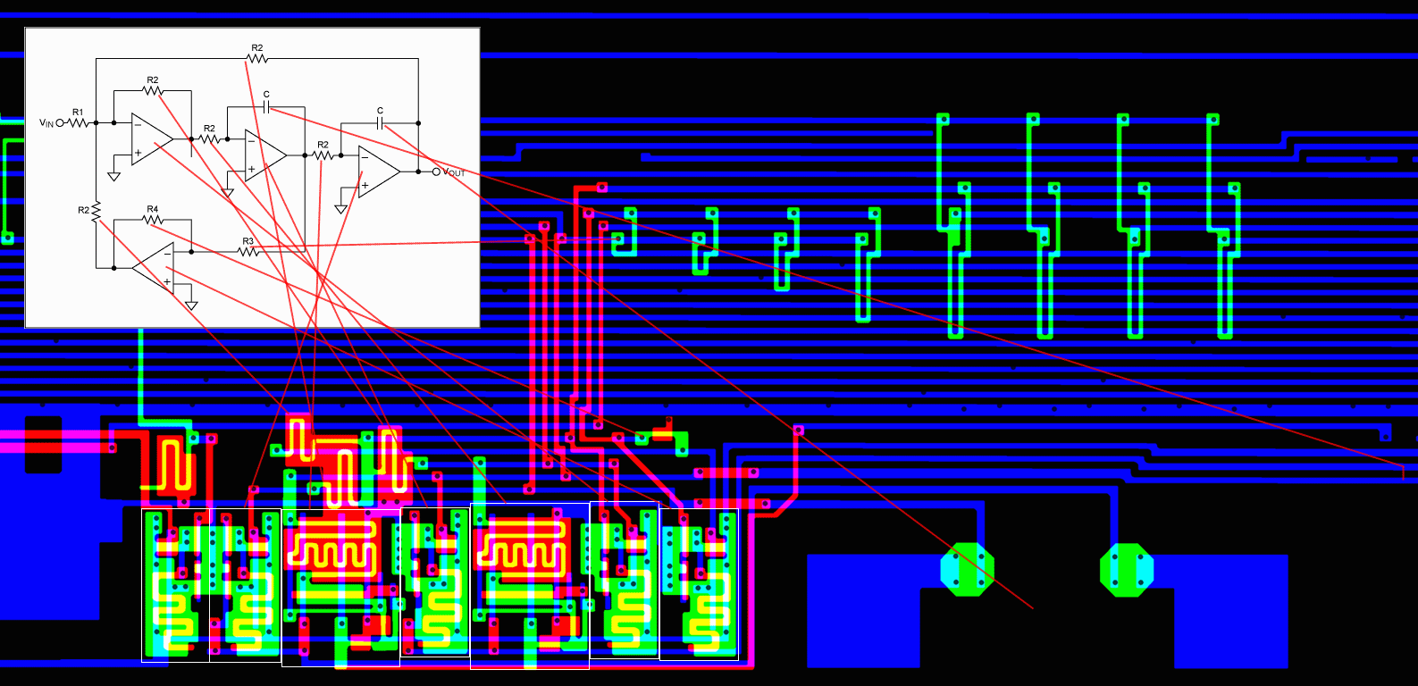
Tried to draw a schematic for the 6581 filter section:

Attachment:
6581_filt1.png
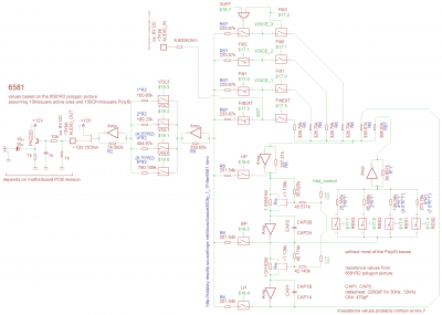
6581_filt1.png [ 101.79 KiB | Viewed 10163 times ]


Putting a voltage divider at the gate of the voltage controlled resistance FETs
is a trick to reduce distortion, I have seen something like that in CD4007 schematics.

Looks like the filter curve will go off with temperature.
Unfortunately, there was no space on the silicon to implement something like
a temperature sensor circuitry which modifies the voltage in the frequency control DAC
to compensate for this... but we are getting there later in the 8580.

;---

Also, I tried to calculate the resistance of the PolySi traces in the filter,
but at some point it became a bit too much, so please don't expect
all of those resistance values to be correct. :)

Attachment:
6581_filt2.png
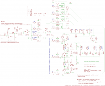
6581_filt2.png [ 127.55 KiB | Viewed 10163 times ]


Anyhow, my reason for calculating the resistances of the PolySi traces only was
to figure out whether they might be big enough to be taken into account or not.

To put it this way:

For a true audiophile who had placed his amplifier on a 1 cubic meter marble block,
hand polished by blind virgins by full moon exactly to the micrometer,
all those resistances probably would matter.

On the other hand, Mr. Joe Average who happens to like Trash Metal
probably won't take a lot of those resistances into account...

just kidding. :lol:

BTW: the schematic doesn't include resistances of the metal traces.
When trying to add them later, please don't forget that metal traces happen to have
a different temperature coefficient than PolySi traces.


Top
 Profile  
Reply with quote  
PostPosted: Wed Sep 14, 2016 10:22 am 
Offline
User avatar

Joined: Fri Nov 09, 2012 5:54 pm
Posts: 1392
The 6581 was manufactured in a 7 micrometer NMOS process.

The 8580 was manufactured in a 2 micrometer HMOS2 process,
means that PolySi and metal resistances will be about 3.5 times bigger
than in the 6581.

Edit: clarification because of BigEd's remark below:
I assume 100Ohms/square for PolySi in the 6581,
and 350Ohms/square for PolySi in the 8580.

;---

Here we go.

8580 analog stuff:

Attachment:
8580_analog.png
8580_analog.png [ 233.39 KiB | Viewed 10151 times ]


Last edited by ttlworks on Wed Sep 14, 2016 10:46 am, edited 1 time in total.

Top
 Profile  
Reply with quote  
PostPosted: Wed Sep 14, 2016 10:37 am 
Offline
User avatar

Joined: Thu Dec 11, 2008 1:28 pm
Posts: 10793
Location: England
Resistances might not go up - it all depends on the square count and the material thickness. (The lines get thinner, but also proportionately shorter, more or less.)


Top
 Profile  
Reply with quote  
PostPosted: Wed Sep 14, 2016 10:39 am 
Offline
User avatar

Joined: Fri Nov 09, 2012 5:54 pm
Posts: 1392
First, we have the waveform DACs.

Picture: MSB of one of the waveform DACs.

Attachment:
s8580_wavdac.png
s8580_wavdac.png [ 13.85 KiB | Viewed 10147 times ]


West: R/2R PolySi resistor ladder of the DAC.

North east: digital DAC buffer for one bit, which gives out 0V or +5V.

South east: Ry, that odd pullup resistor to +5V at the R/2R ladder.

Unlike in the 6581, the output of this ladder is not buffered,
and goes directly to the envelope DAC.

When taking the impedance of the digital DAC buffers into account,
resistor ratio for the DAC ladder is R/1.986R


Top
 Profile  
Reply with quote  
PostPosted: Wed Sep 14, 2016 10:43 am 
Offline
User avatar

Joined: Fri Nov 09, 2012 5:54 pm
Posts: 1392
Schematic for a digital waveform DAC buffer.

Attachment:
8580_wavdac.png
8580_wavdac.png [ 6.13 KiB | Viewed 10147 times ]


Buffer is non_inverting,
and the output either pulls to GND, or gives out +5V.

Note, that the FET which gives out +5V at the output
has a pullup to +9V at the gate.

The inputs of those buffers are fed by the waveform selector switches.


Top
 Profile  
Reply with quote  
PostPosted: Wed Sep 14, 2016 11:14 am 
Offline
User avatar

Joined: Fri Nov 09, 2012 5:54 pm
Posts: 1392
Next, the unbuffered analog signal from the waveform DAC enters the envelope DAC.

The envelope DAC controls the amplitude of the signal.

Picture from the LSB of an envelope DAC:

Attachment:
s8580_envdac.png
s8580_envdac.png [ 20.2 KiB | Viewed 10145 times ]


The digital envelope DAC buffers are controlled by the envelope generator.

Another R/2R PolySi ladder is fed by the digital envelope DAC buffers,
and the analog output of the ladder at the MSB is directly sent
to the selector switches without being buffered.

The 2R end at the LSB of the ladder is tied to ca. 4.759V by a 105.36k resistor
and a ca. 377.8Ohm FET (with +9V at the gate) in series.

That 4.759V voltage is the "vitual ground" in the amplifier\filter section,
we are getting there later.

Schematic for one bit of the digital envelope DAC buffer:

Attachment:
8580_envdac.png
8580_envdac.png [ 5.72 KiB | Viewed 10145 times ]


Odd thing about that buffer is:
If the bit at the buffer input is 1, the buffer connects the output to the signal from the waveform DAC to the output.
If the bit at the buffer input is 0, the buffer connects the output to +4.759V (virtual ground, labeled REF' in my schematic).

Note, that both FETs at the buffer output have a pullup to +9V at the gate.

When taking the output impedance of the digital envelope DAC buffers into account,
resistor ratio for the ladder is R/1.979R


Top
 Profile  
Reply with quote  
Display posts from previous:  Sort by  
Post new topic Reply to topic  [ 164 posts ]  Go to page Previous  1 ... 6, 7, 8, 9, 10, 11  Next

All times are UTC


Who is online

Users browsing this forum: No registered users and 11 guests


You cannot post new topics in this forum
You cannot reply to topics in this forum
You cannot edit your posts in this forum
You cannot delete your posts in this forum
You cannot post attachments in this forum

Search for:
Jump to: