6502.org Forum  Projects  Code  Documents  Tools  Forum
It is currently Sat Apr 27, 2024 10:35 pm

All times are UTC


Post new topic Reply to topic  [ 164 posts ]  Go to page Previous  1 ... 7, 8, 9, 10, 11
Author Message
PostPosted: Wed Sep 21, 2016 5:39 pm 
Offline
User avatar

Joined: Thu Dec 11, 2008 1:28 pm
Posts: 10793
Location: England
aah, I've no idea. I suppose you could try a Google book search, in case some textbook happens to cover these cases.


Top
 Profile  
Reply with quote  
PostPosted: Tue Dec 12, 2017 2:51 pm 
Offline
User avatar

Joined: Fri Nov 09, 2012 5:54 pm
Posts: 1392
Back in 2016, when trying to draw a schematic for the SID envelope DAC counter control, to me the results somehow looked odd.
http://forum.6502.org/viewtopic.php?f=8&t=4150&start=90&sid=687d3f23ffd81b6bd1272a38c77810ec&sid=687d3f23ffd81b6bd1272a38c77810ec#p47184

After gaining some "mental distance" from this adventure, I eventually found the time to dig into that part of the silicon again.

;---

First, a polygon picture with some parts not related to the circuitry to be dissected deleted:

Attachment:
Counting_direction_IC_2.png
Counting_direction_IC_2.png [ 80.78 KiB | Viewed 20346 times ]


;---

Now for what I think that's supposed the equivalent of the circuitry drawn with switches and pullup resistors.

clk1 actually means sid_clk1, same thing for clk2 and sid_clk2.

Switches and resistors are placed in the schematic similar as they are placed in the silicon
Ignore that odd numbering convention, it's just that the chip layout is dense and a bit hard to follow,
so numbering the switches really is helpful for cleaning up the circuitry.

Attachment:
sid_cntdir1.jpg
sid_cntdir1.jpg [ 149.12 KiB | Viewed 20346 times ]


Top
 Profile  
Reply with quote  
PostPosted: Tue Dec 12, 2017 2:54 pm 
Offline
User avatar

Joined: Fri Nov 09, 2012 5:54 pm
Posts: 1392
Attachment:
sid_cntdir2.jpg
sid_cntdir2.jpg [ 155.63 KiB | Viewed 20345 times ]


Attachment:
sid_cntdir3.jpg
sid_cntdir3.jpg [ 129.75 KiB | Viewed 20345 times ]


Attachment:
sid_cntdir4.jpg
sid_cntdir4.jpg [ 120.51 KiB | Viewed 20345 times ]


Attachment:
sid_cntdir5.jpg
sid_cntdir5.jpg [ 118.74 KiB | Viewed 20345 times ]


Looks like my schematic from 2016 is wrong... don't know if my schematic from 2017 is right.


Top
 Profile  
Reply with quote  
PostPosted: Wed Jan 10, 2018 9:27 am 
Offline
User avatar

Joined: Fri Nov 09, 2012 5:54 pm
Posts: 1392
Just a little attempt for translating the envelope circuitry to sort of a TTL equivalent,
sorry for the bad quality of the pictures.

Attachment:
env_log1.jpg
env_log1.jpg [ 88.91 KiB | Viewed 20223 times ]


Attachment:
env_log2.jpg
env_log2.jpg [ 146.15 KiB | Viewed 20223 times ]


Attachment:
env_log3.jpg
env_log3.jpg [ 121.23 KiB | Viewed 20223 times ]


I'm sure, this stuff contains quite some errors, and probably a few of the flipflops could be optimized away.


Top
 Profile  
Reply with quote  
PostPosted: Tue Apr 03, 2018 9:20 pm 
Offline

Joined: Sun Sep 30, 2007 8:38 pm
Posts: 1
Location: Bologna - Italy
ttlworks wrote:
Just a little attempt for translating the envelope circuitry to sort of a TTL equivalent,
sorry for the bad quality of the pictures.
I'm sure, this stuff contains quite some errors, and probably a few of the flipflops could be optimized away.


Hi ttlworks, i like your idea very much. I would like to build a SID wid TTL/CMOS discrete IC.
I use Eagle CAD for my project and if you can help me i can build SID schematic and PCB with CAD.
Waiting for your help,
Luigi.

_________________
Ciao, Luigi.


Top
 Profile  
Reply with quote  
PostPosted: Mon Apr 09, 2018 11:03 am 
Offline
User avatar

Joined: Fri Nov 09, 2012 5:54 pm
Posts: 1392
Hi Luigi,
Sorry for the delay, was on vacation and away from internet.

Just to be fair, I have to say this won't be a small project:
implementing the envelope generators and especially the filter won't be easy.

Would like trying to help you a bit, PM sent,
for this project we better start a new thread in the hardware section of the forum.

;---

Edit: August 21, 2018.
More than 4 months have passed by, and to me it looks like Luigi has lost interest.

Again: building a TTL implementation of the SID won't be a small project,
and when trying to do it "right" this probably could take 3 years+.

So when starting it, you better be serious about "getting the job done".


Top
 Profile  
Reply with quote  
PostPosted: Sun Oct 13, 2019 7:52 pm 
Offline

Joined: Sun Oct 13, 2019 3:19 pm
Posts: 1
I found something interesting that could help in a non-destructive way to reconstruct the SID (if anyone has the $ and inclination)...
[PDF Warning] Computed Laminography for X-ray Inspection of Lightweight Constructions


Top
 Profile  
Reply with quote  
PostPosted: Mon Oct 14, 2019 6:42 am 
Offline
User avatar

Joined: Fri Nov 09, 2012 5:54 pm
Posts: 1392
Hi d3bug, and welcome to the forum.

In theory yes, but the hardware required for X-ray scanning 2 micrometer sized chip structures this way probably would cost more than a new car,
and one would need to have some in_depth knowledge of mechanical construction and machine engineering for building a scanner working at a reasonable precision.
Turning the sensor data into distortion free vectorized images won't be trivial, especially when it comes to manually routed chip layouts.

We had dissected all of the SID circuitry so far, but two mysteries are remaining:
We don't have transfer curves for the FETs in side the chip, so the parameters for the analog part of the SID are "guesswork",
and one month of staring at the microscopic silicon pictures didn't answer the question why the LFSR Bits are flipping from 0 to 1 after a while.

It's questionable if X-raying the SID would bring us far there, but X-raying chips that are no 'mixed signal designs' "in theory" might be interesting.


Top
 Profile  
Reply with quote  
PostPosted: Mon Oct 14, 2019 8:25 am 
Offline
User avatar

Joined: Thu Dec 11, 2008 1:28 pm
Posts: 10793
Location: England
Indeed welcome! There are techniques of lapping which can similarly recover the geometry. But the most labour-intensive step is always the creation of the equivalent polygons - what would have been the original mask data - and debugging any opens or shorts or misconnections.


Top
 Profile  
Reply with quote  
PostPosted: Mon Oct 14, 2019 9:45 am 
Offline
User avatar

Joined: Fri Nov 09, 2012 5:54 pm
Posts: 1392
Nowaday, designers seem to use fancy CAD tools for "cobbling together" a set of "standard cells".

But old MOS\CSG chips (like used in the C64) are manually routed, the designers sure had pulled every dirty trick there is for making the design as compact as possible.
From what I have heard, automated software has problems with generating polygonized images out of something not made from "standard cells",
so the usual approach is to take a microscopic chip picture, then to _manually_ draw the polygonized picture from it by using Inkscape or such...
...for maybe more than 3000 transistors, what sure takes some time (maybe more than 3 months per chip). For more details, see here.

The other thing is, that MOS\CSG seemed to know the one or other thing about the chip manufacturing process (while tinkering with it),
and that knowledge went lost. The blue prints and the original mask data for the chips went lost, too. The old MOS\CSG factory building had an 'existence failure'.
After more than 37 years, the original designers of the chips probably can't remember anymore what they did, and why.

Really, trying to reverse engineer old MOS\CSG chips is a fascinating/entertaining hobby.
Unfortunately, destructive/non_destructive "scanning" of the chip silicon only is one step of a labour intensive process.

Looking forward to seeing somebody building an inexpensive X-ray chip scanner, good luck. :)

Edit:
The X-ray micro-CT scanner project on HaD might be a nice starting point.
When tinkering with X-rays, please don't forget to have an adequate shielding.


Top
 Profile  
Reply with quote  
PostPosted: Mon Oct 14, 2019 2:50 pm 
Offline

Joined: Thu Jul 20, 2017 9:58 am
Posts: 91
ttlworks wrote:
...
From what I have heard, automated software has problems with generating polygonized images out of something not made from "standard cells",
so the usual approach is to take a microscopic chip picture, then to _manually_ draw the polygonized picture from it by using Inkscape or such...
...for maybe more than 3000 transistors, what sure takes some time (maybe more than 3 months per chip)


Good guess! :) That's approx. the time it took me to polygonize the MOS6509! (Maybe it was a bit less... but not much).


Top
 Profile  
Reply with quote  
PostPosted: Mon Oct 14, 2019 3:28 pm 
Offline
User avatar

Joined: Fri Nov 09, 2012 5:54 pm
Posts: 1392
fhw72 wrote:
Good guess! :) That's approx. the time it took me to polygonize the MOS6509! (Maybe it was a bit less... but not much).
I know. :)

...plus maybe another three months for making sense and/or partial schematics of the polygonized images (if you know what you are doing),
if the chip doesn't happen to be too complex... like a CPU or such.

Extracting the transistor netlist from the polygonized images by automated software tools for running a simulation might be possible... someday...,
(at least for chips which are not 'mixed signal designs' containing digital plus analog functionality like the SID,)
but that won't be too helpful for trying to figure out how the chip actually works "as a whole" in all of the little details.
You need to understand what's inside the chip by making use of your own brain... and this might involve paper, pencil, and a lot of spare time.

LFSR based counters, FET switches creatively making use of trace capacitances for implementing transparent latches, and so on.


Top
 Profile  
Reply with quote  
PostPosted: Wed Apr 15, 2020 8:21 am 
Offline
User avatar

Joined: Fri Nov 09, 2012 5:54 pm
Posts: 1392
Since Drass is away for a while, I have tried to "translate" some of the results of our SID dissection into sort of a conceptual TTL schematic.

Pre_Farnell Eagle 6.4, because I happen to have the full version and I'm used to it (as in "drawing goes faster this way").
Attachment:
SID_8580_TTL_ConceptualSchematics.zip [277.27 KiB]
Downloaded 177 times

Edit: sid_main.sch, page 7:
Looks like something went wrong with the notation of the signal names: A0..A4, should be _A0.._A4, sorry.
Anyhow, it's only a "test balloon".

;---

Decided to aim for the 8580, because I lack some info for implementing the 6581 filter.
Nevertheless, resistor values in the waveform selectors are like in the 6581, take care.
Schematics are _not_ verified, and I shouldn't try to do a verification because I'm too deep into these schematics.
Would be better to check if 'PHI11' and 'PHI22' are assigned correctly to the circuitry.
Schematics might contain some errors, and I wouldn't trust the envelope control circuitry too much.
Really, you better question/doubt anything in the schematics. Take them with a grain of salt.

Couldn't resist "to try making the bus interface 20MHz", because we have that 20MHz TTL CPU.
Of course, the oscillator\envelope logic probably won't be able to go faster than 2MHz,
running the design with two phase_synchronous PHI2 clocks (registers 20MHz, oscillator\envelope 1MHz)
might create some _other_ problems...
...also, because there probably won't be enough PCB space for even thinking about double buffering the control registers.

It's going to be a stack of four PCBs:
Three identical PCBs for the voices (oscillator + envelope + the related DACs), //3* 105 ICs
One PCB containing the bus interface, the filter and the rest. //1* 56 ICs

Since the schematics are not verified, it doesn't make sense to spend any thoughts yet on if/how that stuff might be going to fit on the PCBs,
371 ICs in total, have fun.

;---

Bus interface, with the wrong sort of connectors of course:
Attachment:
sid_main.png
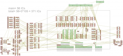
sid_main.png [ 187.94 KiB | Viewed 14171 times ]


One voice, three such PCBs required. //Note the massive use of BAS40-05 and BAS40-06 Schottky diodes.
Attachment:
sid_voice.png
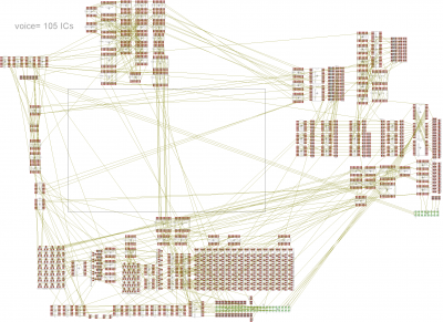
sid_voice.png [ 347.52 KiB | Viewed 14171 times ]

It's a beauty... at least to fans of Boris Karloff.

;---

Edit:
After some tinkering with the 'voice' schematics and PCB layout, I would dare to say that there is no way to squeeze this into a 160mm * 100mm form factor.
I'm sorry to say this... but maybe we should spend some thoughts about an alternative concept.

Attachment:
sid_voice2.png
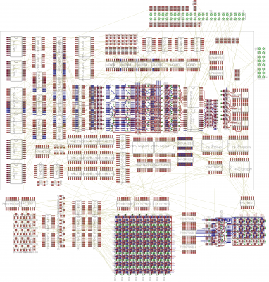
sid_voice2.png [ 1.04 MiB | Viewed 13998 times ]


Top
 Profile  
Reply with quote  
PostPosted: Wed Jul 27, 2022 9:48 pm 
Offline

Joined: Wed Jul 27, 2022 9:27 pm
Posts: 5
Bit late to the party.
I don't think anyone mentioned here yet why the noise LFSR magically turns to all-1s when you keep the test bit set.

Each bit in the noise LFSR has three pass transisors, LC (copying the nomenclature that was already used here), that is used to shift in the neighboring bit, and c1 and c2, used to refresh the register.
When the test bit is set, LC is ON and c1 and c2 are OFF.
That means that the contents of the bits won't be refreshed, so the bits of poly that come off c1 gradually lose charge, and the inverter connected to it will become 1 after some time.


Attachments:
File comment: noise LFSR bits
IMG_20220727_234412989.jpg
IMG_20220727_234412989.jpg [ 15.62 KiB | Viewed 13529 times ]
Top
 Profile  
Reply with quote  
Display posts from previous:  Sort by  
Post new topic Reply to topic  [ 164 posts ]  Go to page Previous  1 ... 7, 8, 9, 10, 11

All times are UTC


Who is online

Users browsing this forum: No registered users and 10 guests


You cannot post new topics in this forum
You cannot reply to topics in this forum
You cannot edit your posts in this forum
You cannot delete your posts in this forum
You cannot post attachments in this forum

Search for:
Jump to: