6502.org Forum  Projects  Code  Documents  Tools  Forum
It is currently Mon Apr 29, 2024 7:13 am

All times are UTC


Post new topic Reply to topic  [ 164 posts ]  Go to page Previous  1, 2, 3, 4, 5, 6, 7, 8 ... 11  Next
Author Message
PostPosted: Mon Jul 18, 2016 1:28 pm 
Offline
User avatar

Joined: Fri Nov 09, 2012 5:54 pm
Posts: 1392
Oscillator register, even bits:
Attachment:
osc_latch_even.png
osc_latch_even.png [ 12.85 KiB | Viewed 8270 times ]


Oscillator register, odd bits:
Attachment:
osc_latch_odd.png
osc_latch_odd.png [ 13.56 KiB | Viewed 8270 times ]


;---

Frequency register, even bits:
Attachment:
freq_latch_even.png
freq_latch_even.png [ 10.19 KiB | Viewed 8270 times ]


Frequency register, odd bits:
Attachment:
freq_latch_odd.png
freq_latch_odd.png [ 10.27 KiB | Viewed 8270 times ]


Odd thing is, that the SID really has three 8 bit frequency registers per oscillator channel.
When the CPU writes a byte into frequency register latches bit 15..8,
frequency register latches bit 23..16 are written with '0'.


Top
 Profile  
Reply with quote  
PostPosted: Mon Jul 18, 2016 1:31 pm 
Offline
User avatar

Joined: Tue Jun 07, 2016 4:34 pm
Posts: 53
BigEd wrote:
The width and length of a transistor directly relates to on-resistance, so it sounds like the 8-series part has a weighting function applied to the inputs - does that fit the facts?


Ah yes, I can see a reason for this. When both triangle and sawtooth switches are active the current will flow mostly to the output as the sawtooth transistor is bigger, offering less resistance. This way, if the noise switch is active too, there would be less chances for feedback into the LFSR reducing the risk for lockups. And the lower four bits are not connected to the noise register so those would not cause any problem.
Still I can't explain the wider transistors...

I think that the muffled sound for combined waveforms and noise lockups were two of the problems that Rob Yannes tried to address in the newer chip model.


Top
 Profile  
Reply with quote  
PostPosted: Mon Jul 18, 2016 2:00 pm 
Offline
User avatar

Joined: Thu Dec 11, 2008 1:28 pm
Posts: 10793
Location: England
Is there any general knowledge that the relative loudness of the triangle vs the sawtooth changed when the chip changed from 6-series to 8-series?


Top
 Profile  
Reply with quote  
PostPosted: Mon Jul 18, 2016 2:49 pm 
Offline
User avatar

Joined: Tue Jun 07, 2016 4:34 pm
Posts: 53
As far as I can remeber there is no mention of something like this anywhere. I can try to make some samplings and see if there is a difference of amplitudes between waveforms. But I'm wondering... isn't the signal still digital at this point?


Top
 Profile  
Reply with quote  
PostPosted: Mon Jul 18, 2016 3:21 pm 
Offline
User avatar

Joined: Thu Dec 11, 2008 1:28 pm
Posts: 10793
Location: England
Oh - maybe it is!


Top
 Profile  
Reply with quote  
PostPosted: Tue Jul 19, 2016 10:26 am 
Offline
User avatar

Joined: Fri Nov 09, 2012 5:54 pm
Posts: 1392
Generation of osc_rst drawn a bit different:
Attachment:
osc_rst1.png
osc_rst1.png [ 9.94 KiB | Viewed 8233 times ]


Generation of osc_rst, this time with logic gates:
Attachment:
osc_rst2.png
osc_rst2.png [ 16.85 KiB | Viewed 8233 times ]


V3 is bit 23 from oscillator 3 latch which goes into
osc_rst generation of oscillator 1:
Attachment:
osc_bit23.png
osc_bit23.png [ 7.57 KiB | Viewed 8233 times ]


I now feel a need to mention that the inverters I did draw at the outputs
of the oscillator odd bit latches actually are located at the north east
corner of an oscillator adder cell, decided to draw it this way
because IMHO this is helpful to understand the adder from the
logic design point of view.

Quote:
This means that the oscillator is reset when test bit is set or when sync bit is set
and the sync source voice's MSB switches from low to high.

Exactly like that.


Top
 Profile  
Reply with quote  
PostPosted: Tue Jul 19, 2016 10:29 am 
Offline
User avatar

Joined: Fri Nov 09, 2012 5:54 pm
Posts: 1392
Now to take a look at the pulse width stuff.

Pulse with latches, even bits:
Attachment:
pw_latch_even.png
pw_latch_even.png [ 9.74 KiB | Viewed 8231 times ]


Pulse with latches, odd bits:
Attachment:
pw_latch_odd.png
pw_latch_odd.png [ 8.63 KiB | Viewed 8231 times ]


The pulse width comparators are nothing but a carry chain
like in the 7480... with the sum logic missing, of course.
Attachment:
pw_carry.png
pw_carry.png [ 15.89 KiB | Viewed 8231 times ]


The concept goes like this:
the adder does osc_23..12 + /pw_11..0 + 1.
Means, the carry input of the lowest bit of the adder is tied to 5V.

Because pw_11..0 is inverted before it is passed into the adder
(ones complement), and we also add 1, the adder calculates
osc_23..12 - pw_11..0.

The CMP instruction in the 6502 works somewhat similar,
so the carry output of that adder carry chain is
'0', if osc_23..12 < pw_1..0.
Else, it is '1'.

Generation of 'pulse':
Attachment:
pw_pulse.png
pw_pulse.png [ 14 KiB | Viewed 8231 times ]


If carry=1, or if test=1, then pulse=1 (what would set the DAC to $FFF).


Top
 Profile  
Reply with quote  
PostPosted: Tue Jul 19, 2016 10:43 am 
Offline
User avatar

Joined: Tue Jun 07, 2016 4:34 pm
Posts: 53
Did a sampling of the output of both chips for every possible waveform. Selecting the noise along with other type of waves produces no output so the pictures show only the following combinations:

  1. Triangle
  2. Sawtooth
  3. Triangle+Sawtooth
  4. Pulse
  5. Triangle+Pulse
  6. Sawtooth+Pulse
  7. Triangle+Sawtooth+Pulse
  8. Noise

6581:
Attachment:
Waves_6581.PNG
Waves_6581.PNG [ 12.01 KiB | Viewed 8231 times ]


8580:
Attachment:
Waves_8580.PNG
Waves_8580.PNG [ 8.48 KiB | Viewed 8231 times ]


There is no substantial difference in the amplitude between Triangle and Sawtooth in the 8580. It is interesting to note however that combinations which include both Sawtooth and Triangle are much louder in the newer model and that there is a small DC drift when passing from wave 5 to 6 in the 6581.

In other news I've fitted the transistor list into the perfect6502 emulation engine and the results look good, confirming the validity of the work done so far :). There is only one of the three voices implemented and the emulation covers only the digital behaviour of transistors. If anyone want to have a look the code is available in the libsidplayfp repository (https://sourceforge.net/p/sidplay-resid ... rfect6581/)


Top
 Profile  
Reply with quote  
PostPosted: Tue Jul 19, 2016 10:52 am 
Offline
User avatar

Joined: Thu Dec 11, 2008 1:28 pm
Posts: 10793
Location: England
Thanks for publishing your code - more transistor-level modelling is always a good thing!


Top
 Profile  
Reply with quote  
PostPosted: Tue Jul 19, 2016 12:54 pm 
Offline
User avatar

Joined: Fri Nov 09, 2012 5:54 pm
Posts: 1392
Generation of TriXOR:
Attachment:
trixor.png
trixor.png [ 12.82 KiB | Viewed 8224 times ]

From the logic design point of view, it looks like V3 really gets inverted there...
but I don't know, why.

Generation of the Saw_bits:
Attachment:
saw_bits.png
saw_bits.png [ 31.8 KiB | Viewed 8224 times ]


Top
 Profile  
Reply with quote  
PostPosted: Wed Jul 20, 2016 2:45 pm 
Offline
User avatar

Joined: Fri Nov 09, 2012 5:54 pm
Posts: 1392
Now for the bus interface.

First the circuitry which generates the internal inverted and non_inverted address lines
Ax_low and Ax_high from the external Ax address bus.
It makes creative use of super buffers:
Attachment:
sid_ax1.png
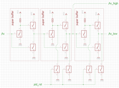
sid_ax1.png [ 19.72 KiB | Viewed 8197 times ]


From the logic design point of view, it's something like this:
Attachment:
sid_ax2.png
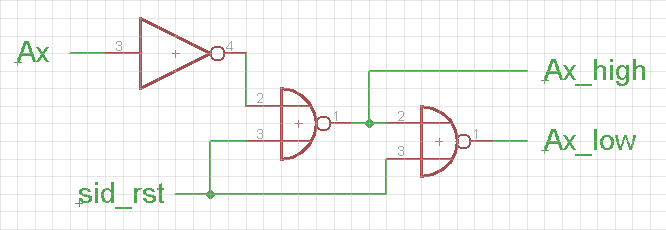
sid_ax2.png [ 6.83 KiB | Viewed 8197 times ]


If sid_rst = 1, then Ax_high = 0 and Ax_low = 0.
Else, Ax_high = Ax and AX_low = /Ax.

;---

The circuitry which generates /read and /write also makes creative use of super buffers:
Attachment:
sid_csrw1.png
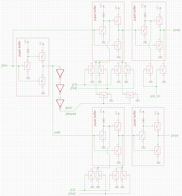
sid_csrw1.png [ 31.61 KiB | Viewed 8197 times ]


Logic design point of view:
Attachment:
sid_csrw2.png
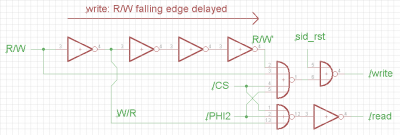
sid_csrw2.png [ 13.22 KiB | Viewed 8197 times ]


For write cycles, the falling edge of R/W is delayed.
//Considering the C64 bus timing, it would be interesting to compare the 6522 and 6526 bus interface...

Note, that /write is forced to '0' if sid_rst = 1.

When taking a look at the data bus buffers later, it becomes evident that the internal data bus
is forced to $00 while sid_rst = 1.

So during a RESET, if sid_rst = 1, all the NOR address decoder gates tied to /write
will go active because all their address inputs are 0.
This forces a write of $00 into _all_ of the registers that could be written from the bus.

Nice trick.

;---

Now a code snippet from vice 2.4 > resid > resid.cc
Code:
// Write registers.
// Writes are one cycle delayed on the MOS8580. This is only modeled for
// single cycle clocking.
// ----------------------------------------------------------------------------
void SID::write(reg8 offset, reg8 value)
{
  write_address = offset;
  bus_value = value;
  bus_value_ttl = 0x4000;

  if (sid_model == MOS8580) {
    // One cycle pipeline delay on the MOS8580; delay write.
    write_pipeline = 1;
  }
  else {
    // No pipeline delay on the MOS6581; write immediately.
    write();
  }
}


But after dissecting the bus interface circuitry of 6581R3 and 8580R5,
I'd say that the bus interfaces just have different geometries,
but they seem to be identical at transistor level from the
logic design point of view.

In other words: we were unable to find any proof that there might be something
like a one cycle write delay on the 8580.

;---

Also, vice 2.4 resid source code implicates, that when writing a register,
the byte also stays on the internal data bus, and if you try to read a register
that can't be read you are just "getting that byte back".

But after $2000..$4000 clock cycles, bits that were 1 on the internal data bus
are "fading" to 0.

BTW: don't get confused by the overly simplified schematics from the logic point of view above,
they are just there to show how things are working in general.
Trying to build a 6502 compatible bus interface for a peripheral chip can give you some grey hairs,
especially when trying to aim for speed.

When I did an experimental TTL implementation of the 6522... but I'm getting off topic. :)


Top
 Profile  
Reply with quote  
PostPosted: Wed Jul 20, 2016 4:03 pm 
Offline
User avatar

Joined: Fri Nov 09, 2012 5:54 pm
Posts: 1392
Buffer from external data bus Dx to internal data bus DBx for writing registers:
Note, that sid_rst = 1 places $00 on the internal data bus DBX if /write = 0
for writing all registers that can be written from the bus with $00 at RESET.
Attachment:
sid_Dx_to_DBx.png
sid_Dx_to_DBx.png [ 22.18 KiB | Viewed 8191 times ]


;---

Buffer from internal data bus DBx to external data bus Dx for reading registers:
Attachment:
sid_DBx_to_Dx.png
sid_DBx_to_Dx.png [ 40.96 KiB | Viewed 8191 times ]


Top
 Profile  
Reply with quote  
PostPosted: Wed Jul 20, 2016 4:31 pm 
Offline
User avatar

Joined: Fri Nov 09, 2012 5:54 pm
Posts: 1392
The register which reads the upper 8 Bits of the Osc 3 DAC output:
Attachment:
sid_osc3_read.png
sid_osc3_read.png [ 21.57 KiB | Viewed 8188 times ]


;---

One bit of the three control registers:
Attachment:
sid_latch_ctl.png
sid_latch_ctl.png [ 8.09 KiB | Viewed 8188 times ]


IMHO they just had to build it that way because capacitive load on the CTLx lines could be big...
if a CTLx line drives 12 waveform switches, for instance.
I think the flipflop won't work reliable when connecting CTLx directly to the output
of the second inverter which holds the bit in the flipflop if sid_clk1 = 1.


Top
 Profile  
Reply with quote  
PostPosted: Thu Jul 21, 2016 8:28 am 
Offline
User avatar

Joined: Fri Nov 09, 2012 5:54 pm
Posts: 1392
Now for the DAC buffer:
It's a _digital_ non_inverting buffer,
built from a normal inverting buffer and an inverting super buffer.

Means, we could assume that the buffer gives out either nearly 0V, or nearly 5V.
"Nearly" depends on the on_resistance of the FETs at the output and the output current.

For the input, I think we could assume a treshold between 0.8V..2.0V,
where "treshold" is the turning point between low and high.
Attachment:
6581_dacbuffer.png
6581_dacbuffer.png [ 9.04 KiB | Viewed 8167 times ]


;---

Waveform selectors:
Evil. Eeevil...
Attachment:
6581_waveselect.png
6581_waveselect.png [ 54.18 KiB | Viewed 8167 times ]


In the 8580, osc_23 is buffered by a flipflop before it enters that "Sawtooth" switch.

In the 6581, it is not.
The Pulse line which is switched to the DAC buffer inputs in pulse width mode
has a push/pull output, while everything else that could be switched to the
DAC buffer inputs just has a pullup plus an open drain FET switching to GND as an output.

Means, on the 6581, it might be possible that if the "Sawtooth" and "Pulse"
selector switches are closed, the Pulse line might probably override the output
of the osc_23 flipflop... causing _really_ odd effects.

;---

BTW: in the 6581 and the 8580, the noise selector switches really connect to
the LFSR bits 0,2,5,9,11,14,18,20 in the same order. Checked this...


Top
 Profile  
Reply with quote  
PostPosted: Thu Jul 21, 2016 10:01 am 
Offline
User avatar

Joined: Tue Jun 07, 2016 4:34 pm
Posts: 53
ttlworks wrote:
Means, on the 6581, it might be possible that if the "Sawtooth" and "Pulse"
selector switches are closed, the Pulse line might probably override the output
of the osc_23 flipflop... causing _really_ odd effects.

One of those nasty side effects is that if the pulse is pulling the output low it will force a zero in the oscillator's adder MSB even if the bit is high, thus resetting the top bit in the following cycle.


Top
 Profile  
Reply with quote  
Display posts from previous:  Sort by  
Post new topic Reply to topic  [ 164 posts ]  Go to page Previous  1, 2, 3, 4, 5, 6, 7, 8 ... 11  Next

All times are UTC


Who is online

Users browsing this forum: No registered users and 6 guests


You cannot post new topics in this forum
You cannot reply to topics in this forum
You cannot edit your posts in this forum
You cannot delete your posts in this forum
You cannot post attachments in this forum

Search for:
Jump to: