6502.org Forum  Projects  Code  Documents  Tools  Forum
It is currently Sun Apr 28, 2024 8:28 pm

All times are UTC


Post new topic Reply to topic  [ 164 posts ]  Go to page Previous  1, 2, 3, 4, 5, 6, 7 ... 11  Next
Author Message
PostPosted: Mon Jun 27, 2016 11:55 am 
Offline
User avatar

Joined: Fri Nov 09, 2012 5:54 pm
Posts: 1392
Thanks for marking those transistors.
Tried to draw white lines around the flipflops for bit 0 and bit 1:

Attachment:
lfsr_flip.png
lfsr_flip.png [ 46.36 KiB | Viewed 8557 times ]


Top
 Profile  
Reply with quote  
PostPosted: Tue Jun 28, 2016 10:20 am 
Offline
User avatar

Joined: Tue Jun 07, 2016 4:34 pm
Posts: 53
Yes, that's correct, and there are seven transistors per bit, no pull-up/pull-down resistor to avoid floating state. Also I'm noticing that the oscillator is not tied to the reset signal even if it is supposed to be zeroed out at startup. :?

Anyway I started looking at the address bus as suggested.
There are five address pins, from A0 to A4, to allow indexing the 29 chip registers.

Attachment:
Address_pin_IC.png
Address_pin_IC.png [ 33.17 KiB | Viewed 8537 times ]


Again some big transistors to control timings, but basically this produces two signals, one of which is high when the line is high and the other when it's low. During reset both signals are held at zero.

Attachment:
Address_pin.png
Address_pin.png [ 19.63 KiB | Viewed 8537 times ]


Top
 Profile  
Reply with quote  
PostPosted: Thu Jun 30, 2016 4:21 pm 
Offline
User avatar

Joined: Tue Jun 07, 2016 4:34 pm
Posts: 53
These are two address decoders for the read-only register $1B (OSC3) on the left and the write-only register $12 (CR3) on the right.

Attachment:
Address_decoders_IC.png
Address_decoders_IC.png [ 25.62 KiB | Viewed 8478 times ]


Each decoder just NORs the five address lines and the read/write line, taking as input either the active low or the active high ones depending on the register's address and function. A register is therefore activated when all of its inputs are low.

Attachment:
Address_decoders.png
Address_decoders.png [ 9.3 KiB | Viewed 8505 times ]


For example the line $1B is active only when the address bus has the value 11011, so if one or more of the A4_low, A3_low, A2_high, A1_low or or A0_low lines are high the decoder outputs a zero. This also happens, being a read-only register, when the write line is high.

This is the full map of the address decoders:

Attachment:
address_bus.png
address_bus.png [ 257.37 KiB | Viewed 8514 times ]


The description of the registers is available here from the reference manual.


Edit: updated schematic.
Edit2: updated line names in the layout.


Last edited by drfiemost on Fri Jul 01, 2016 2:13 pm, edited 1 time in total.

Top
 Profile  
Reply with quote  
PostPosted: Fri Jul 01, 2016 8:00 am 
Offline
User avatar

Joined: Fri Nov 09, 2012 5:54 pm
Posts: 1392
Looks like the adders tied to the oscillator registers
are nothing but a NMOS implementation of the bipolar TTL 7480.

More info about the 7480 can be found here:
http://6502.org/users/dieter/a5/a5_3.htm

;---

Hmm...
so if the frequency tuning word of an oscillator would be $0000,
the oscillator (phase accumulator) would stop running ?

This brings up an interesting question:

When clearing the bits in the LFSR somehow,
then instantly setting the frequency tuning word to $0000
for stopping the oscillator... and the LFSR clock too...
would the bits in the LFSR still flip back to 1 after a while ?

If they would stay 0, the "magic" for bringing those bits back to 1
probably isn't hidden in the bits 0, 2, 5, 9, 11, 14, 18 and 20
of the LFSR. :mrgreen:


Top
 Profile  
Reply with quote  
PostPosted: Fri Jul 01, 2016 10:27 am 
Offline
User avatar

Joined: Tue Jun 07, 2016 4:34 pm
Posts: 53
If the oscillator stops the LFSR won't be shifted anymore but it should still retain its value, as the C1 and C2 gates would be closed. Only the reset and test lines can reset the noise register.
However I might test this case just out of curiosity.


Top
 Profile  
Reply with quote  
PostPosted: Fri Jul 01, 2016 3:14 pm 
Offline
User avatar

Joined: Tue Jun 07, 2016 4:34 pm
Posts: 53
Here is the last bit for the address decoding, the CS and R/W pins. CS is the active low chip select signal while R/W controls the data flow direction.
More details on the pins and the timings can be found in the reference

Attachment:
CS_RW_IC.png
CS_RW_IC.png [ 53.99 KiB | Viewed 8476 times ]


Both the read and write operations are controlled through NOR gates using the CS, Phi2 and RW signals as input.

Attachment:
CS_RW.png
CS_RW.png [ 42.03 KiB | Viewed 8476 times ]


The resulting expressions are:
/Write = ¬(¬(RW ∨ ¬Phi2 ∨ /CS ∨ _RW) ∨ sid_rst) = (RW ∨ ¬Phi2 ∨ /CS ∨ _RW) ∧ ¬sid_rst
/Read = ¬(¬(/CS ∨ ¬Phi2 ∨ A)) = /CS ∨ ¬Phi2 ∨ ¬RW

where _RW is the RW signal slightly delayed by passing through a few inverters, maybe to give the data bus some time before doing the actual writing.

The read/write operations are then done when CS is low and Phi2 is high. When RW is high a read is performed otherwise it's a write.
During reset the /Write line is low while /Read is high, meaning that every register is written to as we have seen that all the address lines are low too.
I guess this is used to zero out all the registers at startup, but we need to have a look at the data bus before concluding that. Another interesting thing to find out is what happens when reading from a write-only or from a non-existing register.


Top
 Profile  
Reply with quote  
PostPosted: Tue Jul 05, 2016 2:47 pm 
Offline
User avatar

Joined: Tue Jun 07, 2016 4:34 pm
Posts: 53
This is one of the eight data pins, the input logic on the left and the output logic on the right.

Attachment:
Data_pin_IC.png
Data_pin_IC.png [ 116.6 KiB | Viewed 8455 times ]


The input circuitry is based on NOR ports driven by the /Write and sid_rst signals:

Attachment:
Data_pin_write.png
Data_pin_write.png [ 18.2 KiB | Viewed 8455 times ]


The value at the gates of the two transistors on the right side of the picture (a being the one connected to Vcc and b the one connected to GND) are described by the following expressions:

a = ¬(¬(¬(¬Dx ∨ sid_rst)) ∨ /write) = Dx ∧ ¬sid_rst ∧ ¬/write
b = ¬(¬(¬Dx ∨ sid_rst) ∨ /write) = ¬(Dx ∧ ¬sid_rst) ∧ ¬/write

where Dx is the xth bit pin. The resulting truth table is then:

Code:
Dx sid_rst /write | a b | DBx
------------------|-----|-----
0     0       0   | 0 1 |  0
1     0       0   | 1 0 |  1
0     1       0   | 0 1 |  0
1     1       0   | 0 1 |  0
0     0       1   | 0 0 |  x
1     0       1   | 0 0 |  x
0     1       1   | 0 0 |  x
1     1       1   | 0 0 |  x


When the /write line is high the input is disconnected from the data bus, otherwise the data from the pins is written to it, unless the sid_rst signal is high in which case a zero is forced unto the data bus.
This confirms that during a reset all the writeable registers are initialized to zero.
Writing to a read-only or a non-existant register only puts the input value on the data bus.


The output is based on NAND ports driven by the /Read signal:

Attachment:
Data_pin_read.png
Data_pin_read.png [ 18.21 KiB | Viewed 8455 times ]


The value at the gates of the two transistors on the right are described by the following expressions:

a = ¬(¬(DBx ∧ ¬/read)) = DBx ∧ ¬/read
b = ¬(¬(¬DBx ∧ ¬/read)) = ¬DBx ∧ ¬/read

where DBx is the data bus bit x. The resulting truth table is then:

Code:
DBx /read | a b | Dx
----------|-----|-----
0     0   | 0 1 |  0
1     0   | 1 0 |  1
0     1   | 0 0 |  x
1     1   | 0 0 |  x


When the /read line is high the output is disconnected from the data pin, otherwise the value on the data bus can be read from the data pins.
Reading from a write-only or a non-existant register returns the value present on the data bus, which is the one from the last valid read/write. According to the comments in the resid sources this value fades to zero after some time, depending on the chip model and temperature.

At first glance I didn't notice any difference in the 8580 layout apart from the clock logic so I'm unable to explain the one cycle delay for writes :?


Top
 Profile  
Reply with quote  
PostPosted: Wed Jul 06, 2016 3:22 pm 
Offline
User avatar

Joined: Tue Jun 07, 2016 4:34 pm
Posts: 53
Let's have a look at a couple of registers before getting back to the wave generation.

This is one bit from OSC3, a read-only register which allows access to the upper eight bits of the third voice's waveform.

Attachment:
OSC3_bit_IC.png
OSC3_bit_IC.png [ 10.28 KiB | Viewed 8436 times ]


The waveform bits are latched at sid_clk1 and pushed to the databus when the register's line is activated from the address decoder.

Attachment:
OSC3_bit.png
OSC3_bit.png [ 7.46 KiB | Viewed 8436 times ]


The following is from the voice 1 control register.

Attachment:
Control_register_IC.png
Control_register_IC.png [ 11.87 KiB | Viewed 8436 times ]


The databus bits are latched when the register's line is activated. At sid_clk1 the value is forwarded to the components that need it and is also fed back into the latch to keep the bit alive. The curious thing is that the inverted value is sent out and then passed through another inverter, why couldn't this be avoided?

Attachment:
Control_register.png
Control_register.png [ 8.52 KiB | Viewed 8436 times ]


There is another thing that makes me wonder here: why are the /read and /write lines clocked at /Phi2 (or actually a slightly delayed version) and not sid_clk2?


Top
 Profile  
Reply with quote  
PostPosted: Thu Jul 07, 2016 1:29 pm 
Offline
User avatar

Joined: Tue Jun 07, 2016 4:34 pm
Posts: 53
Now on to the wave generation, today we look at the pulse.
This waveform is obtained by comparing the upper 12 bits of the oscillator with a programmable Pulse Width value and setting all the output bits to zero or one depending on the result of the comparison.
In this picture we can see the Pulse Width register bit on the right and an adder's carry-block on the left.

Attachment:
PulseBit_IC.png
PulseBit_IC.png [ 15.31 KiB | Viewed 8418 times ]


The PulseWidth register bits are formed by a couple of inverters where the feedback loop is clocked by sid_clk1. The input is taken from the data bus and is enabled by the $2 line for the low eight bits and $3 for the others.

Attachment:
PulseWidth.png
PulseWidth.png [ 14.74 KiB | Viewed 8350 times ]


The carry calculator is the same as the one in the oscillator adder, with the inverted logic for the even bits.
In order to perform a subtraction the two's complement of the pulse width value is used as input. The pw bits are taken inverted and the carry input (Cin) for the first bit is connected to Vcc (logical 1).

Attachment:
Carry.png
Carry.png [ 15.55 KiB | Viewed 8350 times ]


the resulting expression, as we have already seen, is:

/Cout = ¬((bit_x ∧ PW_x) ∨ (Cin ∧ (bit_x ∨ PW_x)))

The output of the last carry calculator is then used to generate the pulse output, unless the test bit is set.

Attachment:
Pulse_IC.png
Pulse_IC.png [ 10.84 KiB | Viewed 8418 times ]


The carry output is latched at sid_clk2 and NORed with the test bit. The result is latched at sid_clk1 and used, after an inversion, for the pulse bits.

Attachment:
Pulse.png
Pulse.png [ 8.59 KiB | Viewed 8418 times ]


When the test bit is set the pulse output is fixed at $fff.


Edit: fixes


Last edited by drfiemost on Wed Jul 13, 2016 3:24 pm, edited 1 time in total.

Top
 Profile  
Reply with quote  
PostPosted: Sat Jul 09, 2016 9:23 am 
Offline
User avatar

Joined: Tue Jun 07, 2016 4:34 pm
Posts: 53
drfiemost wrote:
The carry output is latched at sid_clk2 and NORed with the test bit. The result is latched at sid_clk1 and used, after an inversion, for the pulse bits.

Just to add that the latching, as noted in the resid comments, causes a one cycle delay in the pulse waveform with respect to the oscillator value.
Also I'm wondering if I have to swap the sid_clk1 and sid_clk2 labels, as it will look more logical to me...

By the way, I've updated the clocking scheme again, now it _really_ makes sense.


Top
 Profile  
Reply with quote  
PostPosted: Mon Jul 11, 2016 2:30 pm 
Offline
User avatar

Joined: Tue Jun 07, 2016 4:34 pm
Posts: 53
Next one is the triangle waveform.
The upper 12 bits of the oscillator run from 0 to $fff, at a speed dependent on the frequency, producing a sawtooth waveform.
A triangle waveform is obtained by XORing the bits with the oscillator's MSB, in this way during the second half of the wave, when the MSB is 1, the bits are inverted forming the descending ramp of the triangle. As the result is only 11 bits the value is shifted to the left and the LSB is set to 0, thus halving the resolution but retaining full amplitude.
It is possible to apply a ring modulation effect, controlled by Bit 2 of the Control Register, so the MSB is XORed with the (inverted) MSB of the preceeding voice producing non-harmonic overtones.
This is the XOR logic applied to the first eleven bits of the oscillator's output:

Attachment:
Tri_bit_IC.png
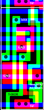
Tri_bit_IC.png [ 9.09 KiB | Viewed 8370 times ]


The output results from the following expression:
Tri_bitX = ¬((TriXOR ∧ bitX) ∨ ¬(TriXOR ∨ bitX))
= TriXOR + bitX

Attachment:
Tri_bit.png
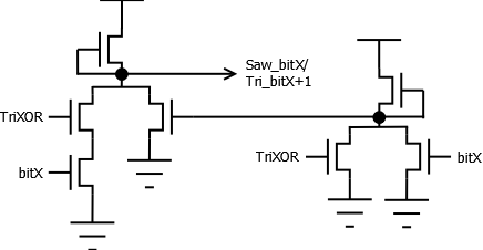
Tri_bit.png [ 7.44 KiB | Viewed 8370 times ]


The xor input is generated by the following circuit:

Attachment:
Triangle_XOR_IC.png
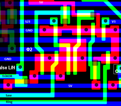
Triangle_XOR_IC.png [ 16.72 KiB | Viewed 8370 times ]


The output results from the following expression:
TriXOR = ¬(a ∨ Saw ∨ (b ∧ bit23))
= ¬Saw ∧ ¬a ∧ ¬(b ∧ bit23)

where:
a = ¬(b ∨ bit23)
b = ¬(V3 ∨ ¬Ring) = ¬V3 ∧ Ring
(V3 is the 23rd bit of the ring modulating voice's oscillator)

resulting in:
TriXOR = ¬Saw ∧ (b ∨ bit23) ∧ ¬(b ∧ bit23)
= ¬Saw ∧ (b + bit23)
= ¬Saw ∧ ((¬V3 ∧ Ring) + bit23)

Attachment:
Triangle_XOR.png
Triangle_XOR.png [ 12.66 KiB | Viewed 8370 times ]


So TriXOR is high for the following combinations:

Code:
S | b23 | V3 | R
--|-----|----|--
0 |  1  | 0  | 0
0 |  1  | 1  | 0
0 |  0  | 0  | 1
0 |  1  | 1  | 1


In other words if the sawtooth waveform is not selected the oscillator bits are inverted when ring modulation is diabled and the MSB is 1 or when ring modulation is enabled and the two MSBs, from the current and the modulating voices, are equal.
When the sawtooth is selected the XORing is disabled as the same output is used for both waweforms.

An interesting thing is that in resid the V3 value is not inverted, so either I've found a bug or I did some mistake. That's something worth exploring :)


Top
 Profile  
Reply with quote  
PostPosted: Thu Jul 14, 2016 2:25 pm 
Offline
User avatar

Joined: Tue Jun 07, 2016 4:34 pm
Posts: 53
Ah, found something really interesting!
While looking at the 8580 IC I noticed that the triangle bits are quite different, taking up more space with a couple more transistors:

Attachment:
Trianlge_bit_8580.png
Trianlge_bit_8580.png [ 7.66 KiB | Viewed 8349 times ]


Let's see what's going on here:

Attachment:
Tri_bit_8580.png
Tri_bit_8580.png [ 15.48 KiB | Viewed 8349 times ]


There is only one logical port surrounded by a few inverters. The result is the same but the intermediate (inverted) value is latched at sid_clk2.

/Tri_bitX = ¬((¬bitX ∧ TriXOR) ∨ (¬bitX ∧ ¬TriXOR))
= ¬(TriXOR + bitX)

I start suspecting that it is only the sawtooth/triangle output that is delayed one cycle and not the register writes.

There is also a difference in how the sawtooth's MSB is obtained:

Attachment:
bit23_8580.png
bit23_8580.png [ 8.56 KiB | Viewed 8349 times ]


In the 6581 the MSB of the oscillator, used as input for the triangle xor logic and the pulse adder last bit, is connected directly to the waveform selector, while in the 8580 it is instead latched at sid_clk2 before being forwarded to the selector.

Attachment:
bit23_8580.png
bit23_8580.png [ 6.86 KiB | Viewed 8349 times ]


This has an implication on combined waveforms: in the 8580 if the sawtooth MSB is pulled down it won't affect the pulse and triangle xor circuits.


Top
 Profile  
Reply with quote  
PostPosted: Mon Jul 18, 2016 12:40 pm 
Offline
User avatar

Joined: Tue Jun 07, 2016 4:34 pm
Posts: 53
I've already introduced the waveform selector in a previous post but I'll add some more details here.
There are twelve bits each with four inputs for the different waveforms connected as follows:

  • Pulse: each bit is connected to the latched output of the pulse adder;
  • Noise: the lower four bits are grounded while the others are connected respectively to the bits 0, 2, 5, 9, 11, 14, 18 and 20 of the LFSR register;
  • Triangle: the LSB is grounded while the remaining bits are connected to the triangle xor outputs;
  • Sawtooth: the lower eleven bits are connected to the triangle xor outputs while the MSB is connected to bit 23 of the oscillator, directly in the 6581 and through a latch in the 8580.

An interesting thing to note is that in the 8580 the upper eight triangle selector transistors are narrower than the others while the lower four and the sawtooth ones are slightly wider. In the 6581 all selector transistors are the same size.

Attachment:
Waveform_selector_8580_IC.png
Waveform_selector_8580_IC.png [ 11.27 KiB | Viewed 8316 times ]


The output of the multiplexer is then passed through what I think is an op-amp before going to the DAC.

Attachment:
Voice_bit_IC.png
Voice_bit_IC.png [ 7.57 KiB | Viewed 8316 times ]


Attachment:
Voice_bit.png
Voice_bit.png [ 6.28 KiB | Viewed 8316 times ]


Last edited by drfiemost on Mon Jul 18, 2016 1:08 pm, edited 1 time in total.

Top
 Profile  
Reply with quote  
PostPosted: Mon Jul 18, 2016 12:42 pm 
Offline
User avatar

Joined: Thu Dec 11, 2008 1:28 pm
Posts: 10793
Location: England
The width and length of a transistor directly relates to on-resistance, so it sounds like the 8-series part has a weighting function applied to the inputs - does that fit the facts?


Top
 Profile  
Reply with quote  
PostPosted: Mon Jul 18, 2016 1:25 pm 
Offline
User avatar

Joined: Fri Nov 09, 2012 5:54 pm
Posts: 1392
Back from vacation... looks like I'm falling behind a little bit. ;)
Sorry for unexpectedly bumping in...

Oscillator adders, re_drawn with switches:
Attachment:
7480_sid1.png
7480_sid1.png [ 15.05 KiB | Viewed 8310 times ]


Oscillator adders, SID versus 7480:
Attachment:
7480_sid2.png
7480_sid2.png [ 21.24 KiB | Viewed 8310 times ]


A screenshot from a Fairchild 7480 datasheet to confirm this:
http://www.mirrorservice.org/sites/www.bitsavers.org/pdf/fairchild/_dataBooks/1978_Fairchild_TTL_Data_Book.pdf
page 177 (4-94)
Attachment:
7480_fairchild.png
7480_fairchild.png [ 83.93 KiB | Viewed 8310 times ]


IMHO the oscillator adders have to be wired up this way to make it work:
(4 adderes shown)
Attachment:
7480_sid_chain.png
7480_sid_chain.png [ 13.58 KiB | Viewed 8310 times ]


Top
 Profile  
Reply with quote  
Display posts from previous:  Sort by  
Post new topic Reply to topic  [ 164 posts ]  Go to page Previous  1, 2, 3, 4, 5, 6, 7 ... 11  Next

All times are UTC


Who is online

Users browsing this forum: No registered users and 6 guests


You cannot post new topics in this forum
You cannot reply to topics in this forum
You cannot edit your posts in this forum
You cannot delete your posts in this forum
You cannot post attachments in this forum

Search for:
Jump to: