6502.org Forum  Projects  Code  Documents  Tools  Forum
It is currently Mon Apr 29, 2024 12:03 am

All times are UTC


Post new topic Reply to topic  [ 164 posts ]  Go to page Previous  1, 2, 3, 4, 5, 6 ... 11  Next
Author Message
PostPosted: Thu Jun 16, 2016 8:34 am 
Offline
User avatar

Joined: Fri Nov 09, 2012 5:54 pm
Posts: 1392
SID_CLKx generation, again another try.
Attachment:
sid_clk10.png
sid_clk10.png [ 33.09 KiB | Viewed 6854 times ]


SID_CLKx generation drawn more simple:
Attachment:
sid_clk11.png
sid_clk11.png [ 22.56 KiB | Viewed 6854 times ]


SID reset:
Attachment:
sid_rst.png
sid_rst.png [ 4.23 KiB | Viewed 6854 times ]


Edit, Edit2: fixed some errors... I think.


Last edited by ttlworks on Tue Jul 19, 2016 3:24 pm, edited 2 times in total.

Top
 Profile  
Reply with quote  
PostPosted: Thu Jun 16, 2016 1:10 pm 
Offline
User avatar

Joined: Fri Nov 09, 2012 5:54 pm
Posts: 1392
In the LFSR clock generator which generates C1,C2,LC from clk,
"Phi2" seems to be SID_CLK2 instead.

;---

The clk generator...
you rotated the screenshot from the chip counter_clockwise by 90 deg, _did_ you ?... :mrgreen:
;
Switch for bit 19 seems to be controlled by SID_CLK2 instead of "Phi2".
The next switch seems to be controlled by SID_CLK1 instead of "Reset".
This makes the left half of your transistor level schematic a master_slave flipflop which stores bit 19
for delaying it one clock cycle.
;
The delayed bit 19 signal (phase accumulator) from the flipflop then goes through
another switch controlled by SID_CLK2 instead of "Phi2", then goes through that inverter,
followed by another switch before entering that AND gate...
was not able to figure out where the control signal for that switch comes from,
but it probably ain't Phi2 again...
;)
BTW: that AND gate still seems to be an edge detector for the delayed bit 19.
;
The /Reset input of the NOR gate which generates clk actually seems to be sid_rst,
which is HIGH (synchronized by SID_CLK1 indeed) when the /RES pin of the chip is LOW\ACTICE,
forcing clk to LOW during a reset.
;
For figuring out _why_ clk seems to be low during a reset,
we need to dig a bit deeper into the LFSR clock generator and the LFSR flipflops again, sorry.


Top
 Profile  
Reply with quote  
PostPosted: Thu Jun 16, 2016 9:19 pm 
Offline
User avatar

Joined: Tue Jun 07, 2016 4:34 pm
Posts: 53
ttlworks wrote:
you rotated the screenshot from the chip counter_clockwise by 90 deg, _did_ you ?... :mrgreen:

Yes, I tried to better fit the images :oops:

Quote:
was not able to figure out where the control signal for that switch comes from,
but it probably ain't Phi2 again...
;)

This is the schematic with the correct signals, the lines in the reference layout were misleading:
Attachment:
LFSR_clk.png
LFSR_clk.png [ 14.78 KiB | Viewed 7016 times ]


Quote:
For figuring out _why_ clk seems to be low during a reset,
we need to dig a bit deeper into the LFSR clock generator and the LFSR flipflops again, sorry.

Well, this matches with the fact that clk is grounded when the test bit is high, as both should reset the LFSR.


Top
 Profile  
Reply with quote  
PostPosted: Fri Jun 17, 2016 6:45 am 
Offline
User avatar

Joined: Fri Nov 09, 2012 5:54 pm
Posts: 1392
Attachment:
lfsr_clock.png
lfsr_clock.png [ 96.5 KiB | Viewed 7001 times ]

LFSR clock looks much better now.

But the schematics implicate, that only one '1' bit is shifted into the LFSR during a reset.


Top
 Profile  
Reply with quote  
PostPosted: Fri Jun 17, 2016 10:23 am 
Offline
User avatar

Joined: Tue Jun 07, 2016 4:34 pm
Posts: 53
ttlworks wrote:
But the schematics implicate, that only one '1' bit is shifted into the LFSR during a reset.

That's part of the mystery I'd like to see through. By empirical observations, sampling the eight outputs readable from the osc3 SID register, it happens that after some time (in the order of 15 to 30 milliseconds on a warm chip) the bits goes high in an orderly fashion, from lower bit to higher (with some exceptions) on 6581 and from the middle to the outside on the 8580. So it seems there is some analog magic going on here... or maybe it has to do with the OSC3 register?

By the way, to end up the noise generator here is the XOR feedback:
Attachment:
LFSR_xor.png
LFSR_xor.png [ 31.99 KiB | Viewed 6986 times ]


The output results from the following expression:
bit0 = ¬((ns17 ∧ a) ∨ b) = ¬(ns17 ∧ a) ∧ ¬b

where:
a = (sid_rst_clk2 ∨ test_clk2 ∨ ns22)
b = ¬(ns17 ∨ a)

resulting in:
bit0 = ¬(ns17 ∧ a) ∧ (ns17 ∨ a) = ns17 ⊕ A = ns17 ⊕ (sid_rst_clk2 ∨ test_clk2 ∨ ns22)


Top
 Profile  
Reply with quote  
PostPosted: Fri Jun 17, 2016 10:36 am 
Offline
User avatar

Joined: Fri Nov 09, 2012 5:54 pm
Posts: 1392
Quote:
By empirical observations, sampling the eight outputs readable from the osc3 SID register,
it happens that after some time (in the order of 15 to 30 milliseconds on a warm chip)
the bits goes high in an orderly fashion, from lower bit to higher (with some exceptions)
on 6581 and from the middle to the outside on the 8580.
So it seems there is some analog magic going on here...
or maybe it has to do with the OSC3 register?

...or with _reading_ the OSC3 register ? ;)
Can't figure out yet, what brings the bits back to 'high' again.

Attachment:
lfsr_in.png
lfsr_in.png [ 11.34 KiB | Viewed 6983 times ]


Another mystery is, how the LFSR input is supposed to be '1' at reset.
Because when feeding '1' XOR 'LFSR bit 17' into the LFSR input,
and 'LFSR bit 17' was 1 by accident, the LFSR input would be '0'.


Top
 Profile  
Reply with quote  
PostPosted: Fri Jun 24, 2016 9:53 am 
Offline
User avatar

Joined: Tue Jun 07, 2016 4:34 pm
Posts: 53
ttlworks wrote:
Can't figure out yet, what brings the bits back to 'high' again.

During reset C1 is closed so the input for the bit's second inverter is floating. Maybe it discharges after some time ending up outputting a 1... but then why the 1 forced into the xor feedback?

While thinking on it I'm decoding the remaining parts of the voice generators so more stuff is coming soon. I've also updated the Phi2 transistor schematic with a small fix and some cleanup.


Top
 Profile  
Reply with quote  
PostPosted: Sun Jun 26, 2016 8:34 am 
Offline
User avatar

Joined: Tue Jun 07, 2016 4:34 pm
Posts: 53
Let's have a look at how the other waveforms are generated. It all begins with a 24 bit phase accumulationg oscillator, described previously by ttlworks.
Here is one of the bits, the Frequency register on the right and a ripple-carry adder on the left. Even bits have inverted logic to save some silicon and speed up the carry chain.

Attachment:
Oscillator_bit_IC.png
Oscillator_bit_IC.png [ 30.05 KiB | Viewed 6932 times ]


The freq register bits are formed by a couple of inverters where the feedback loop is clocked by sid_clk1.
The input is taken from the data bus for the lower 16 bits while upper 8 bits are grounded. The input is enabled by the $0 line for the low eight bits and $1 for the others.
The $0 and $1 lines come from the address bus and I suppose these are enabled at sid_clk2, we'll have a look at this later.

Attachment:
Freq.png
Freq.png [ 17.61 KiB | Viewed 6932 times ]


Then there is a ripple-carry adder which performs the summing of the oscillator value and the freq register.

This is the circuit that calculates the inverted sum:

Attachment:
Osc_adder.png
Osc_adder.png [ 11.4 KiB | Viewed 6932 times ]


And this one calculates the inverted carry:

Attachment:
Osc_carry.png
Osc_carry.png [ 7.59 KiB | Viewed 6932 times ]


resulting in the following expressions:
/S = ¬((osc_x ∧ freq_x ∧ Cin) ∨ (/Cout ∧ (osc_x ∨ freq_x ∨ Cin))
/Cout = ¬((osc_x ∧ freq_x) ∨ (Cin ∧ (osc_x ∨ freq_x)))

which I haven't been able to simplify, but the truth table confirms that it works as expected:

Code:
osc_x freq_x Cin | /Cout | /S
-----------------|-------|---
  0      0    0  |   1   | 1
  0      0    1  |   1   | 0
  0      1    0  |   1   | 0
  0      1    1  |   0   | 1
  1      0    0  |   1   | 0
  1      0    1  |   0   | 1
  1      1    0  |   0   | 1
  1      1    1  |   0   | 0


The resulting sum is latched (inverted for odd bits) at sid_clk2 and then NORed with the osc_rst signal at sid_clk1 producing the output. So when osc_rst is high the oscillator is reset to zero.
The output is sent back to the adder, after passing through an inverter for odd bits. The output of the upper 12 bits is then used for the actual waveform generation.

Attachment:
Osc_bit.png
Osc_bit.png [ 35.55 KiB | Viewed 6932 times ]


Top
 Profile  
Reply with quote  
PostPosted: Sun Jun 26, 2016 8:41 am 
Offline
User avatar

Joined: Tue Jun 07, 2016 4:34 pm
Posts: 53
The osc_rst line is controlled by the following circuit:

Attachment:
Oscillator_rst_IC.png
Oscillator_rst_IC.png [ 27.13 KiB | Viewed 6931 times ]


Attachment:
Oscillator_rst.png
Oscillator_rst.png [ 16.39 KiB | Viewed 6931 times ]


giving the following expression:
osc_rst = ¬(¬test ∧ (¬sync ∨ ¬V3 ∨ V3_prev))
= test ∨ ¬(¬sync ∨ ¬V3 ∨ V3_prev)
= test ∨ (sync ∧ V3 ∧ ¬V3_prev)

where V3 is the MSB of the preceeding voice generator and V3_prev is the value of V3 during the previous clock cycle.
This means that the oscillator is reset when test bit is set or when sync bit is set and the sync source voice's MSB switches from low to high.


Top
 Profile  
Reply with quote  
PostPosted: Mon Jun 27, 2016 7:35 am 
Offline
User avatar

Joined: Fri Nov 09, 2012 5:54 pm
Posts: 1392
In my opinion it would be a good idea to aim at the address decoder now
to figure out which SID register is where on the silicon.

(Orientation: filter section is South.)

North above the LFSR\Oscillator blocks,
we have 29 six_input NOR gates tied to inverted\non_inverted Bits
of the internal address bus, I think that's the read/write decoder
for the 29 registers.

Attachment:
sid_addrdec.png
sid_addrdec.png [ 45.43 KiB | Viewed 6905 times ]


Picture shows the North East corner of the chip,
two address "pins" and three of the NOR gates.

BTW: the bus interface circuitry of the SID probably isn't trivial,
because SID write cycle setup timing is related to the falling
edge of PHI2.

Maybe we could expect some subtle differences when comparing the 6581 and 8580
bus interface circuitry, because from the comments in the resid source code,
the 8580 seems to write registers with 1 cycle delay compared to the 6581.

;---

Edit: vice 2.4 resid source code implicated something like this,
but after dissecting the 6581 and 8580 bus interfaces,
they seemed to be identical at transistor level.


Last edited by ttlworks on Wed Jul 20, 2016 2:49 pm, edited 1 time in total.

Top
 Profile  
Reply with quote  
PostPosted: Mon Jun 27, 2016 8:08 am 
Offline
User avatar

Joined: Fri Nov 09, 2012 5:54 pm
Posts: 1392
The remaining LFSR mysteries...

Putting that three_input OR gate in front of the XOR gate which feeds the LFSR input
certainly won't do for properly initializing the LFSR.

The OR gate would have to be placed between the XOR gate output and the LFSR input,
but I think this would have required a little bit more space on the silicon.

Of course, "the professional approach" would have been to implement a 23 input
NOR gate to force the LFSR input to 1 if all the LFSR flipflops are 0,
but there certainly wasn't enough space on the silicon for something like that.

So in my opinion, whoever did the logic design for the SID was well aware
that the LFSR bits would be turning from 0 to 1 after a while...

;---

Edit: more than two months had passed by since writing this post.
My theory of a "hidden P FET" turned out to be pure nonsense, so I deleted it.

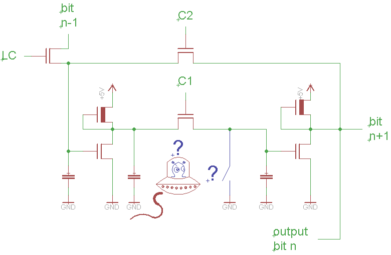
But we still have no clue, what brings the LFSR bits back to '1'
after they were '0' for some time.

1) There is nothing in the transistor level logic design that could explain this effect.

2) When comparing 6581 and 8580, bits seem to go '1' in different order.
// Connections between LFSR and wave selector are wired up identical for both chips, checked this.

3) Effect depends on chip and on temperature.

4) There is nothing "suspicious" in the pictures of the 6581 and 8580 silicon.

Whatever it is, it probably is a trick hidden in the manufacturing process of the silicon or such.
With the info and the skills we have now, we can't solve this riddle.
Attachment:
lfsr_foo.png
lfsr_foo.png [ 7.66 KiB | Viewed 6825 times ]


Last edited by ttlworks on Fri Sep 09, 2016 8:49 am, edited 2 times in total.

Top
 Profile  
Reply with quote  
PostPosted: Mon Jun 27, 2016 8:52 am 
Offline
User avatar

Joined: Thu Dec 11, 2008 1:28 pm
Posts: 10793
Location: England
(Umm, I think this is an NMOS design - there are no P_FETs. Only depletion-mode devices. And they are not invisible, just hard to distinguish from the others.)

But I think I do see 8 transistors in the layout picture of the head post, and only 7 in the circuit diagram, so something seems to be missing.


Top
 Profile  
Reply with quote  
PostPosted: Mon Jun 27, 2016 11:03 am 
Offline
User avatar

Joined: Fri Nov 09, 2012 5:54 pm
Posts: 1392
Thanks, BigEd.
It's just that I'm new to that sort of reverse_engineering...
BigEd wrote:
But I think I do see 8 transistors in the layout picture of the head post, and only 7 in the circuit diagram, so something seems to be missing.

Could you please mark those 8 transistors in the layout picture for us ? :)


Top
 Profile  
Reply with quote  
PostPosted: Mon Jun 27, 2016 11:06 am 
Offline
User avatar

Joined: Thu Dec 11, 2008 1:28 pm
Posts: 10793
Location: England
Anywhere that red crosses green is a transistor. Ignore the blue for this purpose - so the crossing area will be yellow or white.

(But where red touches green with a brown overlay, that's a contact.)


Top
 Profile  
Reply with quote  
PostPosted: Mon Jun 27, 2016 11:38 am 
Offline
User avatar

Joined: Thu Dec 11, 2008 1:28 pm
Posts: 10793
Location: England
Here's an annotated version...
Attachment:
LFSR-annotated.png
LFSR-annotated.png [ 46.32 KiB | Viewed 6883 times ]


Top
 Profile  
Reply with quote  
Display posts from previous:  Sort by  
Post new topic Reply to topic  [ 164 posts ]  Go to page Previous  1, 2, 3, 4, 5, 6 ... 11  Next

All times are UTC


Who is online

Users browsing this forum: dmsc and 6 guests


You cannot post new topics in this forum
You cannot reply to topics in this forum
You cannot edit your posts in this forum
You cannot delete your posts in this forum
You cannot post attachments in this forum

Search for:
Jump to: