Just as the subject suggests... I received a Lab-Volt 6502 Trainer. I'm familiar with the workings of the 6502. However, this trainer isn't exactly intuitive. I'm looking for something like a quick get-started sheet of some kind, so I can start playing around with the unit. My intent is to demonstrate the trainer at the Mini Maker Faire in my area. I already ordered the accompanying book via Amazon, but it is going to take awhile to get to my front door.
Thanks!
Lab-Volt 6502 Trainer - Looking for instructions

Re: Lab-Volt 6502 Trainer - Looking for instructions
Welcome, groinksan. Do you have any photos you can share with us? (They can be included as an attachment with your post -- no need to use a third-party host.) Please also share any links you may've found.
Have you powered up the unit? Does it even have a power supply? Or is that something you'll be required to provide?
cheers,
Jeff
Have you powered up the unit? Does it even have a power supply? Or is that something you'll be required to provide?
cheers,
Jeff
In 1988 my 65C02 got six new registers and 44 new full-speed instructions!
https://laughtonelectronics.com/Arcana/ ... mmary.html
https://laughtonelectronics.com/Arcana/ ... mmary.html
Re: Lab-Volt 6502 Trainer - Looking for instructions
The unit runs great. I had to purchase banana plugs, and modify a 5vDC wall wart with those plugs to get the unit powered (req's 700mA, or more if you have the additional modules.)
The trainer has a 4x4 keyboard. You use it to enter hex, but it also has pre-programmed functions. FWD and BACK upon power up scrolls through memory. If you set the unit to STEP mode, the STEP button will execute code one at at time. Otherwise, I believe with the unit in RUN mode, it'll plow through the code just like any computer. I believe GO will allow you to enter the start address.
As for the layout of the trainer, and so far this is from what I can see on the memory decoder, ROM resides in F000. RAM resides in D000. And, I think the "USER ROM" is in E000.
It also uses the 6520 PIA to output to the display. The display is just six 7-seg display parts, with four for the address bus, and two for the data bus. There are two 20x2 headers, so you can use those to tap into and allow for peripherals, such as a printer or serial interface, or even more RAM. There are other things like an I/O decoder, output data latch, and some LEDs you can blink off/on, but I've yet to figure out how to use those.
- Attachments
-
-

Re: Lab-Volt 6502 Trainer - Looking for instructions
Very nice find groinksan! And welcome.
It would be nice if you could dump the ROM - that will spill all the secrets of what this trainer is capable of.
It's just possible you can get something from the manufacturer, who seems to be Festo or Festo Didactic, who have a North American presence but might actually be from Germany. See
http://www.festo-didactic.com/ov3/media ... tems_1.pdf and also http://www.festo-didactic.com/de-de but I think you'd need to find a nice helpful person with access to materials from obsolete product lines.
It seems that the board was used educationally in Turkey... and in fact as you may know it seems to be allied to the Visual 6502 project of Nurettin Topaloğlu whose site features a photo of this board:
http://w3.gazi.edu.tr/~nurettin/visual_en.html
but, alas, with no further detail. (His Visual 6502 is a GUI simulator for Windows, not to be confused with the in-browser transistor-level simulator at visual6502.org)
Elsewhere, someone notes
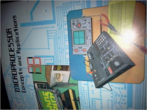
There's a book "Microprocessor Troubleshooting: Concepts and Applications" published by Buck Engineering Company which might cover this Lab Volt board. Or even better, one called "MICROPROCESSOR - CONCEPTS AND APPLICATIONS" by Buck Engineering
which features this board on the cover.
http://www.amazon.com/dp/B002K7TK8Y/
It would be nice if you could dump the ROM - that will spill all the secrets of what this trainer is capable of.
It's just possible you can get something from the manufacturer, who seems to be Festo or Festo Didactic, who have a North American presence but might actually be from Germany. See
http://www.festo-didactic.com/ov3/media ... tems_1.pdf and also http://www.festo-didactic.com/de-de but I think you'd need to find a nice helpful person with access to materials from obsolete product lines.
It seems that the board was used educationally in Turkey... and in fact as you may know it seems to be allied to the Visual 6502 project of Nurettin Topaloğlu whose site features a photo of this board:
http://w3.gazi.edu.tr/~nurettin/visual_en.html
but, alas, with no further detail. (His Visual 6502 is a GUI simulator for Windows, not to be confused with the in-browser transistor-level simulator at visual6502.org)
Elsewhere, someone notes
Quote:
The native language of the software appears to be Turkish, but I found a language setting in an ini file (reversed the order of Turkish/English) and that switched it to English mode. I haven't messed with it too much but it does look pretty cool, and the reason I wanted it was because it has some "virtual" switches and LEDs to play with and supposedly interfaces with my trainer somehow
which features this board on the cover.
http://www.amazon.com/dp/B002K7TK8Y/
Re: Lab-Volt 6502 Trainer - Looking for instructions
I'll see about getting the monitor ROM dumped. I have a ROM reader, so I'll try to get working on that this week.
In the meantime, I've been studying the board. From what I can get out of the memory decoding portion, the memory map looks like this:
$0000 - $0003 - PIA (6520)
$0004 - $CFFF - not recognized by the immediate hardware
$D000 - $D7FF - RAM
$D800 - $DFFF - not recognized by the immediate hardware
$E000 - $EFFF - User ROM
$F000 - $FFFF - Monitor ROM
There are memory cards for this trainer. They're quite hard to find. So I presume those unused portions of memory space can be used by the memory card.
-
GARTHWILSON

- Forum Moderator
- Posts: 8774
- Joined: 30 Aug 2002
- Location: Southern California
- Contact:
Re: Lab-Volt 6502 Trainer - Looking for instructions
groinksan wrote:
There are memory cards for this trainer. They're quite hard to find.
http://WilsonMinesCo.com/ lots of 6502 resources
The "second front page" is http://wilsonminesco.com/links.html .
What's an additional VIA among friends, anyhow?
The "second front page" is http://wilsonminesco.com/links.html .
What's an additional VIA among friends, anyhow?
Re: Lab-Volt 6502 Trainer - Looking for instructions
groinksan wrote:
From what I can get out of the memory decoding portion, the memory map looks like this:
Quote:
There are memory cards for this trainer. They're quite hard to find.
-- Jeff
In 1988 my 65C02 got six new registers and 44 new full-speed instructions!
https://laughtonelectronics.com/Arcana/ ... mmary.html
https://laughtonelectronics.com/Arcana/ ... mmary.html
-
barrym95838

- Posts: 2056
- Joined: 30 Jun 2013
- Location: Sacramento, CA, USA
Re: Lab-Volt 6502 Trainer - Looking for instructions
Dr Jefyll wrote:
... Nowadays you can economically build your own memory expansion (wire-wrap or PCB, as Garth suggests) of any desired capacity (up to 64K) using just a single memory IC.
-- Jeff
-- Jeff
Mike B.
Re: Lab-Volt 6502 Trainer - Looking for instructions
Dr Jefyll wrote:
groinksan wrote:
From what I can get out of the memory decoding portion, the memory map looks like this:
Re: Lab-Volt 6502 Trainer - Looking for instructions
If the memory decoding doesn't use A14 or A15, then everything will get mirrored 4 times on 16k boundaries. But that still doesn't place any RAM over page 0 and 1. Have you perhaps missed an inversion of an address bit?
$0000 is also $4000, $8000 and $C000
$1000 is also $5000, $9000 and $D000
$2000 is also $6000, $A000 and $E000
$3000 is also $7000, $B000 and $F000
(Hope I got that right...)
$0000 is also $4000, $8000 and $C000
$1000 is also $5000, $9000 and $D000
$2000 is also $6000, $A000 and $E000
$3000 is also $7000, $B000 and $F000
(Hope I got that right...)
Re: Lab-Volt 6502 Trainer - Looking for instructions
I found this schematic of the board. The resolution is low, so reading it is difficult.
- Attachments
-
-
barrym95838
- Posts: 2056
- Joined: 30 Jun 2013
- Location: Sacramento, CA, USA
Re: Lab-Volt 6502 Trainer - Looking for instructions
Perhaps a misunderstanding of the silk-screen labeling on the top of the board? It says "RAM (D0-D3)" and "RAM (D4-D7)", but my instincts take that to mean that each RAM is four bits wide ... I'm not a hardware guy, so I could be spouting nonsense.
Mike B.
Mike B.
Re: Lab-Volt 6502 Trainer - Looking for instructions
The 2114 is 1k x 4 bits, and that schematic does appear to show D0-D3 to one chip and D4 to D7 to the other.
The Eprom in the photo looks like a 2k 2516, although the schematic appears to show an option for A11 to be connected for a 4k eprom . The user rom appears to be wired for 4k as well.
So maybe its Ram 0000-03FF with lots of shadows up to 1FFF, User rom 2000-2FFF, monitor rom 3000 - 3FFF then that's repeated 4 times so that there is a monitor rom shadow covering the vectors ?
Re: Lab-Volt 6502 Trainer - Looking for instructions
Hi groinksan are you still investigating this trainer? Do you have the means for dumping and sharing the ROM contents? If not, we can surely write a little program which will output an audio or radio signal carrying the ROM contents, and then decode the result back to binary for investigation. (We can get the output on the address pins, so no need to figure out how to drive the I/O)
(Ref. my puzzle thread, and also this blog post recently mentioned on hackaday.)
(Ref. my puzzle thread, and also this blog post recently mentioned on hackaday.)
Re: Lab-Volt 6502 Trainer - Looking for instructions
I just yesterday received the instructional book. It includes the total breakdown of the memory map, and as I expected I was way off. With the book now in-hand, I can start working on this trainer.