6502.org Forum  Projects  Code  Documents  Tools  Forum
It is currently Sat Jun 08, 2024 7:44 am

All times are UTC


Post new topic Reply to topic  [ 164 posts ]  Go to page Previous  1 ... 3, 4, 5, 6, 7, 8, 9 ... 11  Next
Author Message
PostPosted: Thu Jul 21, 2016 11:26 am 
Offline
User avatar

Joined: Fri Nov 09, 2012 5:54 pm
Posts: 1395
drfiemost wrote:
One of those nasty side effects is that if the pulse is pulling the output low
it will force a zero in the oscillator's adder MSB even if the bit is high,
thus resetting the top bit in the following cycle.

If no carry went into the adder bit 23, that yes. :)
But if the MSB is 0 in the next cycle, the PW logic suddenly might get
a pretty different value and change its output again...
maybe affecting the oscillator MSB again... hmm...

The FET that drives the Pulse line high has only 5V max. at the gate,
so I think it can't source much current, and a NFET switching to GND
might be able to clobber down the voltage at the Pulse line below 0.8V.

;---

But all this brings up some interesting questions:

How much current do those pullup FETs source ?

What's the typical ON resistance of the NFETs which pull a signal to GND ?

What's the resistance of those MonoSi\PolySi traces ?

The PolySi traces between LFSR and waveform selector switches
are shorter than the PolySi traces that make the DAC resistors...
but some of them are not _much_ shorter.

Question to BigEd:
7µm NMOS, I think... ? //correct me if I'm wrong there.
You happen to have any values, thumb rules or approximations at hand by accident ? ;)
...When trying to aim for the filter section later, we probably might need that sort of info anyway.


Top
 Profile  
Reply with quote  
PostPosted: Thu Jul 21, 2016 12:35 pm 
Offline
User avatar

Joined: Thu Dec 11, 2008 1:28 pm
Posts: 10822
Location: England
From memory, poly resistance was something like 50 Ohms per square: you count squares because aspect ratio is all that matters. I've a feeling contact resistance was something like 100, whereas a conducting FET was more like 10k Ohms. Let me see if I have a book... ... I do, Mead & Conway, I open it and goodness that smell takes me back to 1984. They say:
Metal resistance 30 milliOhms per square
Diffusion (Active Area) resistance 10 Ohms per square
Poly resistance 15-100 Ohms per square
FET resistance 10k Ohms per square
(They say tabulated values are typical of 1978 - so they might have changed a bit.)

So my recollection was within an order of magnitude!


Top
 Profile  
Reply with quote  
PostPosted: Thu Jul 21, 2016 2:11 pm 
Offline
User avatar

Joined: Fri Nov 09, 2012 5:54 pm
Posts: 1395
Thanks, BigEd !

Quote:
Poly resistance 15-100 Ohms per square

https://en.wikipedia.org/wiki/Ohms_per_square

Ok, then. Let's see if I got it right:

DAC resistor picture.
6581R2 > OSC1 waveform DAC > Bit0 > R //not 2R.
Attachment:
DAC_R.png
DAC_R.png [ 12.97 KiB | Viewed 5358 times ]

Width = 13 pixels

Length ca. 366 + 24 + 383 + 24 + 398 + 24 + 398 +24 + 362 = 2003 pixels.

2003 / 13 = 154.08

15..100 Ohms per square * 154.08 would be 2.311 kOhms .. 15.408 kOhms for that resistor, right ?


Top
 Profile  
Reply with quote  
PostPosted: Thu Jul 21, 2016 8:08 pm 
Offline
User avatar

Joined: Thu Dec 11, 2008 1:28 pm
Posts: 10822
Location: England
Yes, 15k Ohms if your poly resistance is towards the high end of the range. Are these circuits designed so that absolute resistances matter, or only resistance ratios?

BTW I remember now that it's traditional to count a corner as half a square, not that it makes a lot of difference.


Top
 Profile  
Reply with quote  
PostPosted: Fri Jul 22, 2016 5:44 am 
Offline
User avatar

Joined: Fri Nov 09, 2012 5:54 pm
Posts: 1395
BigEd wrote:
BTW I remember now that it's traditional to count a corner as half a square, not that it makes a lot of difference.

Thanks, BigEd. :)

For a R/2R DAC, it's the resistance ratio that matters of course.
https://en.wikipedia.org/wiki/Resistor_ladder

But I'm not aware about the input capacitance of the circuitry that is fed
by the resistor ladder, and 13 * 15.4 kOhm = 200.2 kOhm isn't exactly
a small resistance value. :)

The resistance of the resistor latter plus the input capacitance
of the circuitry attached to the output of the ladder form a
low pass filter, and I can't judge the cutoff frequency for now.

The lower the DAC bit, the lower the cutoff frequency,
so IMHO when trying to generate a waveform different from
Sawtooth, Triangle and Pulse, maybe it would be a little bit daring
trying to judge from the analog output signal which of the DAC buffers
emit low or high, especially for the lower bits.

Maybe I'm just overly paranoid here... ;)

;---

BTW: from the vice 2.4 resid source code, it seems to be more something like
R/2.2R for the 6581, but it feels like they didn't take the output impedance
of the DAC buffers into account... we are getting there later.

Edit: seems like they did, and I somehow had missed that part when using M$ WordPad.

;---

But back on topic:

An interesting point still is, how much current those pullup FETs may source.

Just to be able to judge how many pullup FETs one NMOS switch to GND could handle
when the drain\source resistance of said switch still keeps the voltage below 0.8V. :)


Last edited by ttlworks on Fri Jul 22, 2016 2:01 pm, edited 1 time in total.

Top
 Profile  
Reply with quote  
PostPosted: Fri Jul 22, 2016 8:40 am 
Offline
User avatar

Joined: Thu Dec 11, 2008 1:28 pm
Posts: 10822
Location: England
According to the book, the input capacitance of a MOSFET is around 0.4fF per square micron - but it's a voltage-variable capacitance.

Rather than thinking of transistors sourcing current, I tend to think of them as having resistance. (I think that might be a reasonable model for FETs, as opposed to conventional bipolar transistors. But it might just be my lack of sophistication!)

In most cases, you'll see pullup resistors with the opposite aspect ratio to pull downs. A pull down might be 4 squares wide, where a pullup might be 4 squares long. So, to a first order, that's a 16:1 ratio of resistances, initially, and a greater ratio as the output voltage is drawn down.

I think you can find an online version of Mead & Conway - it's very readable. Here's a copy, on Lynn Conway's site:
http://ai.eecs.umich.edu/people/conway/ ... -V2/V2.pdf
Page 69 has the table I've been checking.
(She invented the whole approach, AIUI, whereas Mead had the profile to promote it.)


Top
 Profile  
Reply with quote  
PostPosted: Fri Jul 22, 2016 12:40 pm 
Offline
User avatar

Joined: Fri Nov 09, 2012 5:54 pm
Posts: 1395
Many thanks for the link, BigEd.
Reading this will take some time.

...Dang.
It took me a long time to flesh out a concept for building an ALU with multiplexers,
and that book from 1978 comes up with a similar concept on page 196.
If I would have had that link before I had started building my transistor CPU,
this sure would have saved me some trouble. :)


Top
 Profile  
Reply with quote  
PostPosted: Fri Jul 22, 2016 12:42 pm 
Offline
User avatar

Joined: Thu Dec 11, 2008 1:28 pm
Posts: 10822
Location: England
Yes, the Mead&Conway ALU just makes it look so simple and obvious!


Top
 Profile  
Reply with quote  
PostPosted: Fri Jul 22, 2016 1:48 pm 
Offline
User avatar

Joined: Tue Jun 07, 2016 4:34 pm
Posts: 53
ttlworks wrote:
The lower the DAC bit, the lower the cutoff frequency,
so IMHO when trying to generate a waveform different from
Sawtooth, Triangle and Pulse, maybe it would be a little bit daring
trying to judge from the analog output signal which of the DAC buffers
emit low or high, especially for the lower bits.

And the signal passes also through an external filter, unless sampling from the audio out pin directly.
It is however possible to read the digital output from the OSC3 register, even though sacrificing four bits of accuracy. Unfortunately the hard task is to have a cycle accurate sampling. The available data seems to have been measured without accounting for the pulse width so it's quite misleading.

Quote:
BTW: from the vice 2.4 resid source code, it seems to be more something like
R/2.2R for the 6581, but it feels like they didn't take the output impedance
of the DAC buffers into account... we are getting there later.

Actually it mentions that the output impedance may have an effect:
Quote:
In addition to this, the 6581 DACs exhibit further severe discontinuities
for higher bits, which may be explained by a less than perfect match between
the R and 2R resistors, or by output impedance in the NMOS transistors
providing the bit voltages
. A good approximation of the actual DAC output is
achieved for 2R/R ~ 2.20.

There are also some other interesting differences between the two model's DACs beyond the missing terminator and the R/2R ratio, but I'd better go for the evelope generator befor jumping over to the analog parts.


Top
 Profile  
Reply with quote  
PostPosted: Mon Jul 25, 2016 2:23 pm 
Offline
User avatar

Joined: Tue Jun 07, 2016 4:34 pm
Posts: 53
Back to the original question of the noise lockup, I've finally found the answer!

Here's an image depicting two neighbouring bits of the noise register, the first of which is connected to the output.
Attachment:
LFSR_bit_writeback.png
LFSR_bit_writeback.png [ 36.8 KiB | Viewed 5282 times ]


As we have seen the LFSR gates acts as following:
Code:
   | normal | reset/test |  first cycle after
   | cycle  |   shift    | reset/test or shift
---|--------|------------|---------------------
c1 |  high  |    low     |         high
c2 |  high  |    low     |         low
LC |  low   |    high    |         low


So this is what happens when the output is driven low by another waveform if it is mixed with noise:
  • during the normal cycles the output is written back to the bit n through the c2 gate, overwriting its value;
  • during shifting and when test or reset line is active the output is buffered into the first inverter of the next bit n+1 through the LC gate, while the second inverter has the input floating;
  • in the first cycle following the shifting or the releasing of the test/reset line the value stored in the first inverter during the previous cycle is passed through the c1 gate to the second inverter and becomes the actual bit output. No write-back is possible during this cycle as the c2 and LC gates are not active.

Thank you for the help :D
Now on to the remaining SID mysteries!


Top
 Profile  
Reply with quote  
PostPosted: Tue Jul 26, 2016 8:23 am 
Offline
User avatar

Joined: Fri Nov 09, 2012 5:54 pm
Posts: 1395
6581 waveform selectors again.
Attachment:
6581_waveselect_ohm.png
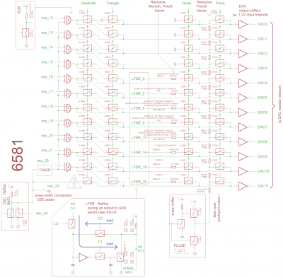
6581_waveselect_ohm.png [ 120.01 KiB | Viewed 5230 times ]

Tried to calculate the resistance values of FETs and traces,
assuming that PolySi has 100 Ohms / square.

From the book:
Code:
Metal      ca. 0.1     Ohms / square
Diffusion  ca. 10      Ohms / square
Poly       ca. 15..100 Ohms / square
Transistor ca. 10k     Ohms / square


Omitted the resistance values of the metal traces,
because they would be 4.2 Ohms or less.

Also, I omitted the Diffusion traces between the selector switches,
because having them in the schematic above wouldn't have increased readability...
Attachment:
6581_waveselect_sw.png
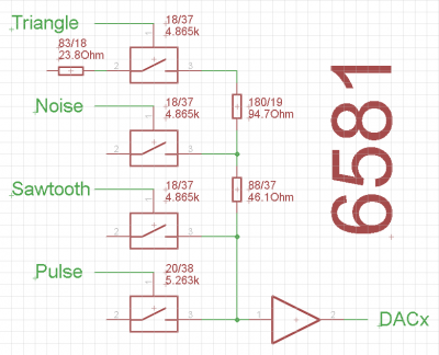
6581_waveselect_sw.png [ 20.3 KiB | Viewed 5230 times ]


All the values are roughly estimated "house numbers" for the 6581R2, of course,
and I'm not sure all of those values might be correct. :)

Would suggest that somebody spends some weeks with dissecting the layouts
of the other 6581 revisions and the 8580 to extract the exact resistance values.

BTW:
When comparing different 6581s, there might be some tolerance in the resistance values.
Tolerance might be bigger when comparing 6581R2s from different batches.
And it still might get bigger when comparing different 6581 revisions.

But I think that for an initial simulation of the waveform mixing effects in a 6581,
the stuff above might do.

;---

Basically, when mixing waveforms, we have resistors to GND and resistors to +5V
(the FET transistors at the outputs of a gate or a flipflop),
and resistors in between (the traces on Poly and Diffusion layer etc.).

For the DAC buffers and the LFSR flipflop inputs, threshold voltage
(turning point from logic level low to logic level high)
is supposed to be ca. 1.2V.

What voltage really is there depends on the resistance values...
but we could suppose, that the bigger the resistance of the traces,
the less good mixing the waveforms may work...

German wikipedia says, that the 8580 was manufactured with a HMOS II process,
and that HMOS II is 2 micrometers (with a typical propagation delay of ca. 30 ns per logic gate.)
https://de.wikipedia.org/wiki/MOS_Technology_SID
https://de.wikipedia.org/wiki/HMOS

6581 had 7 micrometers, so the traces in the 8580 might have 3.5 times
the resistance value of the traces in the 6581, while resistance value
of the FETs for both chips probably would be similar.

...So I guess that mixing waveforms on the 8580 "would sound less impressive"
than on the 6581.

;---

Edit1: Added resistor values to the switches, thanks to BigEd for pointing this out.

Edit2: Pulse selector switches have slightly different geometry, thanks to drfiemost for pointing this out.
Edit2: Added wikipedia link to HMOS II.


Last edited by ttlworks on Wed Jul 27, 2016 5:53 am, edited 2 times in total.

Top
 Profile  
Reply with quote  
PostPosted: Tue Jul 26, 2016 8:39 am 
Offline
User avatar

Joined: Thu Dec 11, 2008 1:28 pm
Posts: 10822
Location: England
It's probably worth modelling the 'on' resistances of the FETs by adding series resistors to the switches - they are likely to be quite substantial.

(Edit: a few extra characters added for clarity)


Top
 Profile  
Reply with quote  
PostPosted: Mon Aug 01, 2016 7:03 am 
Offline
User avatar

Joined: Fri Nov 09, 2012 5:54 pm
Posts: 1395
About calculating the effects of those resistances in and around the waveform selector switches:
I'm not an engineer... but maybe a "star-mesh transform" could help:
https://en.wikipedia.org/wiki/Y-%CE%94_transform

Attachment:
sid_sm1.png
sid_sm1.png [ 22.02 KiB | Viewed 5209 times ]

;---

Maybe this works:
Attachment:
sid_sm2.png
sid_sm2.png [ 30.11 KiB | Viewed 5209 times ]


If we happen to have any electrical engineers or a mathematicians in the forum,
maybe they could come up with a better idea of how to do this... :)


Top
 Profile  
Reply with quote  
PostPosted: Mon Aug 01, 2016 10:08 am 
Offline
User avatar

Joined: Fri Nov 09, 2012 5:54 pm
Posts: 1395
Felt a need to mention, that those resistance values probably are
for 20° Celsius, and that they will change with temperature.

The resistance of the silicon decreases with temperature,
the resistance of the metal traces increases with temperature.

But since we only take the silicon into account and not the metal,
the resistance ratios probably won't change much with temperature,
so I think we safely can ignore (for now) if the chip heats up
to 60° Celsius or so inside the IC package...

https://en.wikipedia.org/wiki/Temperature_coefficient
https://de.wikipedia.org/wiki/Temperaturkoeffizient


Top
 Profile  
Reply with quote  
PostPosted: Thu Aug 11, 2016 7:12 pm 
Offline
User avatar

Joined: Tue Jun 07, 2016 4:34 pm
Posts: 53
Sorry for the lack of updates, I've been working with the VICE guys checking the discoveries on a real C=64. So far most of the findings has been confirmed:

* the ring modulating voice input is actually inverted;

* there is no delay on writes on the 8580;

* the triangle/sawtooth output is delayed half cycle, latched at sid_clk2. This will result in a one cycle delay on the OSC3 registry as this is sampled at sid_clk1.

* reading from a write-only or non-existing register returns the value left on the internal data bus, which is refreshed on writes and on valid reads from the read-only registers.

During the tests we also accidentally noticed that the oscillator has the value 0x555555 at startup (all bits at high, but the odd ones are stored inverted) and is not changed on reset.

I'm still baffled by the 6581 top bit behavior for combined waveforms, hopefully once we jump into the analogic side things will become clearer.

In the meantime work have been ongoing with ttlworks to dissect and understand the envelope generator, more schematics are coming soon, stay tuned!


Top
 Profile  
Reply with quote  
Display posts from previous:  Sort by  
Post new topic Reply to topic  [ 164 posts ]  Go to page Previous  1 ... 3, 4, 5, 6, 7, 8, 9 ... 11  Next

All times are UTC


Who is online

Users browsing this forum: No registered users and 4 guests


You cannot post new topics in this forum
You cannot reply to topics in this forum
You cannot edit your posts in this forum
You cannot delete your posts in this forum
You cannot post attachments in this forum

Search for:
Jump to: