6502.org Forum  Projects  Code  Documents  Tools  Forum
It is currently Sat Apr 27, 2024 7:53 pm

All times are UTC


Post new topic Reply to topic  [ 15 posts ] 
Author Message
 Post subject: Deck65 v2
PostPosted: Wed Jul 26, 2023 8:49 pm 
Offline
User avatar

Joined: Fri Feb 17, 2023 11:59 pm
Posts: 163
Location: Lviv, Ukraine
This is probably a working title since I suck at giving names to things.

Ever since I started playing with 6502 SBCs, I wanted to build a SBC with a 3D-printed or acrylic case, a keyboard, an LCD display and some I/O.

I learned a lot while building multiple revisions of my Deck65 (viewtopic.php?f=12&t=7501&p=98325#p98325), so I'm going to give a try to my larges project so far.

Internals are pretty much unchanged from my Deck65:
- 8 MHz / 2 MHz clock, ATF16V8B
- ACIA (internet access through ESP-01), VIA (I2C, SPI, PS/2 keyboard, GPIO)
- Built-in I2C RTC & I2C EEPROM

However, I'm also adding some new things:
- Built-in 48-key keyboard with Kailh Choc white switches (low-profile, clicky), powered by Atmega328P. Controls the computer through the same PS/2 interface as the external keyboard, can be disabled.
- RAM banking
- A battery would be nice! First I'll need to measure how much current does my beast draw to see if it's going to make sense to add one. But I think I'll have plenty of space for even a really large LiPo battery.

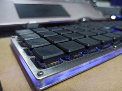
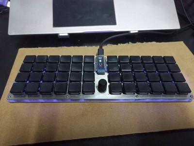
Overall, my goal is to make a fully standalone machine with everything built in, even a keyboard. (I have a lot of experience in building custom mechanical keyboards, I think I've made around 20 so far, mostly hand-wired). Here's my daily driver:
Attachment:
dd1.jpg
dd1.jpg [ 134.21 KiB | Viewed 53320 times ]

Attachment:
dd2.jpg
dd2.jpg [ 154.2 KiB | Viewed 53320 times ]

I love the looks of transparent actylic with stainless steel - maybe eventually my SBC case will look something like it. And besides, making layered cases is very easy, since it's: for example, my keyboard case consists of 5 layers total - top and bottom are stainless steel plates (0.5" thick), and 3 middle layers are transparent acrylic. It also feels very strong and rigid - I think my keyboard can even be used as a blunt weapon!
Also It would probably be cheaper than 3D printing: we have a lot of CNC cutting places in my city, so ordering a custom set of steel or acrylic plates is very cheap (the ones in my keyboard cost me less than $10 to make).

I have experience with 2D CAD, but I really suck at 3D. Seems like FreeCAD is quite powerful and pretty popular, and most importantly - free & open-source. (Last time I did 3D modeling was probably ~18 years ago when me & my friends were making custom maps & mods for Q3 & GoldSrc engine, and probably some gamedev as a hobby several years ago).

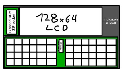
I'm currently thinking about how to make it convenient. I initially thought of having it as a single 10" x 6.3" board (254mm x 160.02mm), but it would probably make sense to have 2 layers (same as most machines of the past - C64, TRS-80 Model 100, etc): main PCB on the bottom and keyboard/LCD at the top. As you might have guessed, Model 100 was a huge inspiration for my build.
Top view
Attachment:
File comment: CORRECTION: 240x64, not 128x64
v2_0_top_view.jpg
v2_0_top_view.jpg [ 29.58 KiB | Viewed 53318 times ]
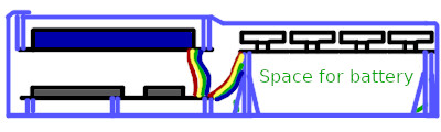
Side view:
Attachment:
v2_0_side_view.jpg
v2_0_side_view.jpg [ 17.64 KiB | Viewed 53320 times ]


JLCPCB estimates 10" x 6.3" at around $11 and I think it's a really nice price.
So I'll probably add a cut to my PCB to split it into two 10" x 3.15" boards.
My current layout looks like this:
Attachment:
v2_0_unrouted.jpg
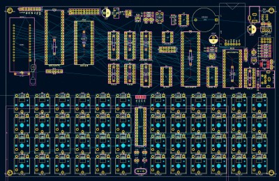
v2_0_unrouted.jpg [ 608.96 KiB | Viewed 53320 times ]

Attachment:
v2_0_3d.jpg
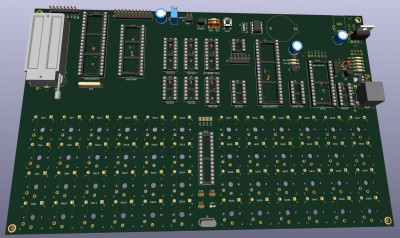
v2_0_3d.jpg [ 287.21 KiB | Viewed 53320 times ]


And once again - Dip Trace is a breeze when it comes to autorouting:
Attachment:
v2_0.jpg
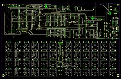
v2_0.jpg [ 502.44 KiB | Viewed 53320 times ]

This is not a final board - just sharing what I've done so far to hear any feedback!

_________________
/Andrew

deck65 - 6502 slab with screen and keyboard | ПК-88 - SBC based on KM1810VM88 (Ukrainian i8088 clone) | leo80 - simple Z80 SBC
nice65 - 6502 assembly linter | My parts, footprints & 3D models for KiCad/FreeCAD


Last edited by and3rson on Sat Sep 16, 2023 10:02 pm, edited 2 times in total.

Top
 Profile  
Reply with quote  
 Post subject: Re: Slab65
PostPosted: Wed Jul 26, 2023 11:35 pm 
Offline

Joined: Fri Mar 18, 2022 6:33 pm
Posts: 432
Neat project! I like the idea of the integrated keyboard. I, too, am just getting started on my most ambitious build so far, and, like you, have a hard time coming up with names. I'm desperately trying to avoid just throwing in the towel and calling it "Blue August." :lol:

_________________
"The key is not to let the hardware sense any fear." - Radical Brad


Top
 Profile  
Reply with quote  
 Post subject: Re: Slab65
PostPosted: Fri Jul 28, 2023 8:04 pm 
Offline
User avatar

Joined: Fri Feb 17, 2023 11:59 pm
Posts: 163
Location: Lviv, Ukraine
Thanks!

"Blue August" actually sounds really nice - you got way more creativity than me, haha!

Some updates: I've ordered the PCB from JLCPCB. I spent two whole days searching for oversights and eventually decided that it still isn't going to work at first try, lol. So I just went for it - my schematic is very similar to my last 6502 SBC, and I think I can fix most new problems with jumper wires anyway.

I also decided to try and do layered case: 2 steel plates (top & bottom) and a bunch of acrylic middle layers with cutouts. It gives me some TI-99/4A vibes:

Attachment:
File comment: Top
v2_0_case_top.png
v2_0_case_top.png [ 41.88 KiB | Viewed 53232 times ]

Attachment:
File comment: Middle
v2_0_case_middle.png
v2_0_case_middle.png [ 18.26 KiB | Viewed 53232 times ]

Attachment:
File comment: Bottom
v2_0_case_bottom.png
v2_0_case_bottom.png [ 78.28 KiB | Viewed 53232 times ]

_________________
/Andrew

deck65 - 6502 slab with screen and keyboard | ПК-88 - SBC based on KM1810VM88 (Ukrainian i8088 clone) | leo80 - simple Z80 SBC
nice65 - 6502 assembly linter | My parts, footprints & 3D models for KiCad/FreeCAD


Top
 Profile  
Reply with quote  
 Post subject: Re: Slab65
PostPosted: Wed Aug 09, 2023 10:52 pm 
Offline
User avatar

Joined: Fri Feb 17, 2023 11:59 pm
Posts: 163
Location: Lviv, Ukraine
PCBs have arrived today!

I still can't believe that nowadays you can get 10" x 6.3" PCB printed for around $11 (and that's for a batch of 5 copies). PCBWay is several times more expensive, so I'm still sticking to JLCPCB.
Shipping was pretty fast, 10 days from China to Ukraine. Last time it took around 3 weeks.

(Sorry for the quality - neither me nor my camera are good at taking photos.)

Attachment:
v2_0_pcb1.jpg
v2_0_pcb1.jpg [ 510.22 KiB | Viewed 53100 times ]


Man, I'm in love with those things, especially matte silkscreens. And the fact that I used my creativity to design them. I usually stare at them for a while before I start soldering, simply admiring how nice they look. This is my first time ordering a PCB with a black silkscreen specifically, and oh boy - isn't it beautiful?!

Attachment:
v2_0_pcb2.jpg
v2_0_pcb2.jpg [ 532.37 KiB | Viewed 53100 times ]


Keyboard is powered with ATmega328P, I've also added an external 16MHz oscillator just in case. However, internal 8MHz oscillator should be totally fine for being a PS/2 driver in my case even though it's very inaccurate, since the timing for PS/2 isn't critical at all. Besides, I'm still reading the PS/2 signal with my VIA, and it doesn't care what the clock frequency is.

Halfway through the soldering process, I noticed that I'm short on keyboard switches... So my keyboard build will have to wait till I get more.

I've tried many different kinds of switches from various vendors over time, and I've settled for Kailh Choc whites. Clicky, 50g actuation force, low profile. I used navies in the past ("thick clicks"), but their 60g of actuation force actually made my fingers much more tired than the whites.

The choice of keycaps is not as broad as with MX-compatible stem, but I use blank keycaps anyway. My favorite profile for Choc switches is MBK, I've been using those caps for past 2 years and I still enjoy their shape with every keypress.

Attachment:
v2_0_pcb3.jpg
v2_0_pcb3.jpg [ 563.53 KiB | Viewed 53100 times ]


As usual, I forgot to use the correct gerber file for silkscreen, so some decals (such as chip orientation and part numbers) are missing. Not a big problem since I have my PCB in front of me in KiCad.

_________________
/Andrew

deck65 - 6502 slab with screen and keyboard | ПК-88 - SBC based on KM1810VM88 (Ukrainian i8088 clone) | leo80 - simple Z80 SBC
nice65 - 6502 assembly linter | My parts, footprints & 3D models for KiCad/FreeCAD


Top
 Profile  
Reply with quote  
 Post subject: Re: Slab65
PostPosted: Fri Aug 11, 2023 10:18 pm 
Offline
User avatar

Joined: Fri Feb 17, 2023 11:59 pm
Posts: 163
Location: Lviv, Ukraine
As I anticipated - I made a really dumb mistake by hard-wiring /OE of my '244 low ('244+'273 act as a RAM banking register) and thus corrupting higher half of the data bus!
Luckily, that was easily fixed by cutting a trace on the PCB. Though to find this mistake, I spent way more time than I'm willing to admit.

Attachment:
v2_0_banking_mistake.jpg
v2_0_banking_mistake.jpg [ 361.55 KiB | Viewed 53054 times ]


I noticed that accidentally hard-wiring an input low when it's supposed to be high (and vice-versa) is not the first time I'm making a mistake and is definitely my trait. Note to future self: always check such things.

On the good side - behold, the build is working, and the keyboard is really nice and works too! I wrote a simple QMK-inspired firmware (since QMK only supports USB HID) that supports multiple layers activated by two layer-shifting keys, thus giving me 3 times more keys (I'm very much used to this setup). All in all, it came out to be pretty simple, only ~200 LOC (not counting the PS/2 scancode definitions): https://github.com/and3rson/deck65/blob ... src/main.c

Attachment:
v2_0_assembled1.jpg
v2_0_assembled1.jpg [ 570.7 KiB | Viewed 53054 times ]

Attachment:
v2_0_assembled2.jpg
v2_0_assembled2.jpg [ 434.64 KiB | Viewed 53054 times ]


By the way, the more I use TL866-II, the more I'm loving it. It's been a nice replacement for a bunch of adapters and I can now program EPROMs, PLDs and AVR MCUs with a single device.
And if I decide to start doing SMD PCBs, I'll just get some PLCC socket adapters for it and still be able to program everything I need.

_________________
/Andrew

deck65 - 6502 slab with screen and keyboard | ПК-88 - SBC based on KM1810VM88 (Ukrainian i8088 clone) | leo80 - simple Z80 SBC
nice65 - 6502 assembly linter | My parts, footprints & 3D models for KiCad/FreeCAD


Top
 Profile  
Reply with quote  
 Post subject: Re: Slab65
PostPosted: Sat Sep 16, 2023 9:57 pm 
Offline
User avatar

Joined: Fri Feb 17, 2023 11:59 pm
Posts: 163
Location: Lviv, Ukraine
Okay, I think I've earned some bragging rights today, so I'll share my success story about 3D modeling with FreeCAD along with some personal excitement.

(I already sent my design files to do a CNC laser cut, but I wanted to have a 3D render of my SBC case while I'm waiting for my order.)

I've been looking with envy at all the amazing projects that people do with FreeCAD. I tried to use Blender once, but it quickly overcame my mental abilities & motivation at that time.

Since I have a lot of experience with LibreCAD (free 2D CAD software), Godot (2D/3D game engine), and I used to do a lot of mapping with Valve Hammer Editor & Milkshape 3D, I finally gave in and spent several hours learning the basics of FreeCAD. And oh boy, it was indeed worth it.

First, I prepared my initial top and bottom "sandwich" plates (as well as acrylic middle layer) with LibreCAD:

Attachment:
top.png
top.png [ 28.55 KiB | Viewed 52742 times ]


I then started importing them into FreeCAD (LibreCAD's DXF export worked perfectly).

I was welcomed by a UI with thousands of buttons, but I felt really determined this time. :D
Attachment:
icons.jpg
icons.jpg [ 123.89 KiB | Viewed 52742 times ]

(Turns out "Arch" is one of the workbenches with several dozen buttons, and there's more than a dozen of workbenches, each with their own unique buttons.)

I spent solid several hours to learn how to extrude the parts. This video helped me a lot (sharing in case someone decides to learn FreeCAD the hard way just as I did): https://www.youtube.com/watch?v=2SF5MUn8HzE
The more I clicked through FreeCAD, the more it clicked in my head. Now, I'm not an expert in FreeCAD by any means: I started just today. Still, I must admit it's an amazing piece of software.

I repeated the same process for middle & bottom layer. At that point, things seemed really neat already - I added some colors and materials:

Attachment:
freecad.jpg
freecad.jpg [ 488.48 KiB | Viewed 52742 times ]


A final small piece was missing: a ray-traced render of the image. Luckily, FreeCAD supports multiple renderers, so I picked POV-Ray since it was available in official Arch Linux package repositories.

After some more tinkering with lights, antialiasing, and materials, I achieved this beauty:

Attachment:
render_angle.jpg
render_angle.jpg [ 75.08 KiB | Viewed 52742 times ]

Attachment:
render_top.jpg
render_top.jpg [ 68.38 KiB | Viewed 52742 times ]


At this point I feel really satisfied with my progress. Learning FreeCAD even at a basic level gave me a new tool that might be invaluable for some of my future projects and allow me to try new things, such as 3D printing.

Finally, I imagined that KiCAD should have an option to export PCB as a 3D model - and it did! So I exported my top PCB half from KiCAD and added it to my FreeCAD project:

Attachment:
editor.jpg
editor.jpg [ 583.47 KiB | Viewed 52741 times ]


After few minutes of rendering, I was blessed with this:

Attachment:
render_angle_pcb.jpg
render_angle_pcb.jpg [ 432.26 KiB | Viewed 52741 times ]

Attachment:
render_top_pcb.jpg
render_top_pcb.jpg [ 426.64 KiB | Viewed 52741 times ]


Beautiful! Isn't it? :oops:

P. S. I decided to rename my project back to "Deck65". I like how it contains several references to old things that I love:
- NES was originally called a "Control Deck"
- My beloved Unreal Tournament 1999 had a map named "Deck 16"
- 65 - what this entire forum is all about!

_________________
/Andrew

deck65 - 6502 slab with screen and keyboard | ПК-88 - SBC based on KM1810VM88 (Ukrainian i8088 clone) | leo80 - simple Z80 SBC
nice65 - 6502 assembly linter | My parts, footprints & 3D models for KiCad/FreeCAD


Top
 Profile  
Reply with quote  
 Post subject: Re: Deck65 v2
PostPosted: Sat Sep 16, 2023 10:52 pm 
Offline

Joined: Fri Jul 09, 2021 10:12 pm
Posts: 741
Very nice! It must be great to be able to see what it will look like when fully assembled! Do you know how much it's costing to make the case, in the end - I think you estimated $11 before, was that right?


Top
 Profile  
Reply with quote  
 Post subject: Re: Deck65 v2
PostPosted: Sat Sep 16, 2023 11:35 pm 
Offline
User avatar

Joined: Fri Feb 17, 2023 11:59 pm
Posts: 163
Location: Lviv, Ukraine
gfoot wrote:
Very nice! It must be great to be able to see what it will look like when fully assembled! Do you know how much it's costing to make the case, in the end - I think you estimated $11 before, was that right?


Thanks! I'm thrilled to see what my final assembly will looked like.
$11 for the PCB, yes. Case cost me ~$16 total for top and bottom plates together (raw materials & laser cutting services). I'll have them ready by Wednesday. We have a lot of local vendors who do steel & acrylic CNC laser cuts, so we get competitive prices. Acrylic middle layers are probably gonna cost slightly more - I'll need ~20mm / 0.8" of clearance, but the thickest ones they can cut are 5mm (IIRC), so I'll have to stack 4 of them.

I initially wanted to place a keyboard at angle (Commodore 64C style), but it requires precise angle calculation for top plate bending, so I'm leaving that for my future attempts.

_________________
/Andrew

deck65 - 6502 slab with screen and keyboard | ПК-88 - SBC based on KM1810VM88 (Ukrainian i8088 clone) | leo80 - simple Z80 SBC
nice65 - 6502 assembly linter | My parts, footprints & 3D models for KiCad/FreeCAD


Top
 Profile  
Reply with quote  
 Post subject: Re: Slab65
PostPosted: Sun Sep 17, 2023 12:18 am 
Offline

Joined: Fri Mar 18, 2022 6:33 pm
Posts: 432
and3rson wrote:
- My beloved Unreal Tournament 1999 had a map named "Deck 16"
You die too easily!

(Deck65 looks great! And also because of cyberdecks, a la Neuromancer, right?)

_________________
"The key is not to let the hardware sense any fear." - Radical Brad


Top
 Profile  
Reply with quote  
 Post subject: Re: Slab65
PostPosted: Tue Oct 03, 2023 11:24 am 
Offline
User avatar

Joined: Fri Feb 17, 2023 11:59 pm
Posts: 163
Location: Lviv, Ukraine
I have a big update: I've assembled the thing and it is... massive. :D

The panels finally arrived today (took longer than usual):

Attachment:
File comment: Bottom panel
case_1_bot.jpg
case_1_bot.jpg [ 1.38 MiB | Viewed 52426 times ]
Attachment:
File comment: Top panel
case_2_top.jpg
case_2_top.jpg [ 1.7 MiB | Viewed 52426 times ]


(I did a really sloopy job polishing them, but I was really losing my patience to see the final assembly)

I used M2 screws for holding everything together.
I started with mounting the PCB:

Attachment:
case_3_pcb.jpg
case_3_pcb.jpg [ 1.25 MiB | Viewed 52426 times ]

(Inner side of the plates could surely use some polishing, but again - I was too impatient!)
I had to add few extra nuts between the plate and the PCB to prevent chip legs from touching the plate (since the plate is made of steel which, as it turns out, is highly conductive! lol)
Attachment:
case_4_screws.jpg
case_4_screws.jpg [ 903.95 KiB | Viewed 52426 times ]


Top assembly looks really neat:
Attachment:
case_5_top.jpg
case_5_top.jpg [ 1.3 MiB | Viewed 52426 times ]
Attachment:
case_6_top_under.jpg
case_6_top_under.jpg [ 1.46 MiB | Viewed 52426 times ]


Final assembly in all its glory:
Attachment:
case_7_assembled.jpg
case_7_assembled.jpg [ 1.43 MiB | Viewed 52426 times ]


The clearance turned out to be almost a whole inch - which is a lot. The major space stealer is a ribbon cable with 26-pin connectors. And the whole thing assembled weights around 3 pounds!
Attachment:
case_8_clearance.jpg
case_8_clearance.jpg [ 811.41 KiB | Viewed 52426 times ]


Finally, I turn it on - and there it goes!
Attachment:
case_9_live.jpg
case_9_live.jpg [ 1.28 MiB | Viewed 52426 times ]


I'm really happy with the result, although it came out kinda bulky. Still, I'm glad I am done with this project - since I started another one while I was waiting for the plates. (Well, technically, it still needs the acrylic middle layers, but that's a job for another day.)

Hope you guys like it!

Paganini wrote:
and3rson wrote:
- My beloved Unreal Tournament 1999 had a map named "Deck 16"
You die too easily!

(Deck65 looks great! And also because of cyberdecks, a la Neuromancer, right?)


Yeah! A whole network of references. :D

_________________
/Andrew

deck65 - 6502 slab with screen and keyboard | ПК-88 - SBC based on KM1810VM88 (Ukrainian i8088 clone) | leo80 - simple Z80 SBC
nice65 - 6502 assembly linter | My parts, footprints & 3D models for KiCad/FreeCAD


Top
 Profile  
Reply with quote  
 Post subject: Re: Deck65 v2
PostPosted: Tue Oct 03, 2023 11:55 am 
Offline
User avatar

Joined: Thu Dec 11, 2008 1:28 pm
Posts: 10793
Location: England
That's great! And surely a useful learning experience, for you and others, as to how one might do things, and what happens. Aiming for thin and light as well as fully functional would be an extra constraint and probably a constraint too far.


Top
 Profile  
Reply with quote  
 Post subject: Re: Deck65 v2
PostPosted: Tue Oct 03, 2023 12:02 pm 
Offline
User avatar

Joined: Fri Feb 17, 2023 11:59 pm
Posts: 163
Location: Lviv, Ukraine
BigEd wrote:
That's great! And surely a useful learning experience, for you and others, as to how one might do things, and what happens. Aiming for thin and light as well as fully functional would be an extra constraint and probably a constraint too far.


Totally! I learned a lot while doing this. Plastic (or 3D-printed case) would be way more practical indeed. Nevertheless, steel was a good option for me since I like the feel of it and it's easier/cheaper to make comparing to plastic. I still wish I had a 3D printer, but owning one means dedicating a lot of time to its steep learning curve.

Also, I just managed to get the clearance down to 0.7" simply by trimming some legs and mounting several resistors on the back side in order to give more space for 26-pin connectors.

Last but not least, FreeCAD has proven to be a great tool for laying out the components - it gives a lot of clarity to how things will stack together.

_________________
/Andrew

deck65 - 6502 slab with screen and keyboard | ПК-88 - SBC based on KM1810VM88 (Ukrainian i8088 clone) | leo80 - simple Z80 SBC
nice65 - 6502 assembly linter | My parts, footprints & 3D models for KiCad/FreeCAD


Top
 Profile  
Reply with quote  
 Post subject: Re: Deck65 v2
PostPosted: Tue Oct 03, 2023 12:52 pm 
Offline

Joined: Fri Mar 18, 2022 6:33 pm
Posts: 432
Boy, that looks great! I like all the little details, like the "stencil" style laser cutout. What's the space between they key islands for (with the crystal and the one IC)?

_________________
"The key is not to let the hardware sense any fear." - Radical Brad


Top
 Profile  
Reply with quote  
 Post subject: Re: Deck65 v2
PostPosted: Tue Oct 03, 2023 6:25 pm 
Offline
User avatar

Joined: Fri Aug 30, 2002 1:09 am
Posts: 8428
Location: Southern California
Wow, really nice!  I've always found packaging to be a huge challenge, in many/most cases greater than the electronics.  Your pictures give me a good idea.

_________________
http://WilsonMinesCo.com/ lots of 6502 resources
The "second front page" is http://wilsonminesco.com/links.html .
What's an additional VIA among friends, anyhow?


Top
 Profile  
Reply with quote  
 Post subject: Re: Deck65 v2
PostPosted: Mon Oct 16, 2023 2:50 pm 
Offline
User avatar

Joined: Fri Feb 17, 2023 11:59 pm
Posts: 163
Location: Lviv, Ukraine
Paganini wrote:
Boy, that looks great! I like all the little details, like the "stencil" style laser cutout. What's the space between they key islands for (with the crystal and the one IC)?

Thanks! I have this space for several reasons:
- It allows me to save some clearance by mounting the IC (in my case - ATmega328P) on the same side as the switches, so the bottom of the board only has diodes.
- Once I started adding this extra space between left and right half in my other keyboards, I got really used to this spacing. It's only extra ~0.8", but my hands feel somewhat more comfortable with this. (I also have several split keyboards, but it's inconvenient to carry them around.)
- Last but not least - I like the naked look of a keyboard controller sticking out like a muscle car engine! :D

_________________
/Andrew

deck65 - 6502 slab with screen and keyboard | ПК-88 - SBC based on KM1810VM88 (Ukrainian i8088 clone) | leo80 - simple Z80 SBC
nice65 - 6502 assembly linter | My parts, footprints & 3D models for KiCad/FreeCAD


Top
 Profile  
Reply with quote  
Display posts from previous:  Sort by  
Post new topic Reply to topic  [ 15 posts ] 

All times are UTC


Who is online

Users browsing this forum: No registered users and 4 guests


You cannot post new topics in this forum
You cannot reply to topics in this forum
You cannot edit your posts in this forum
You cannot delete your posts in this forum
You cannot post attachments in this forum

Search for:
Jump to: