6502.org Forum  Projects  Code  Documents  Tools  Forum
It is currently Sat Apr 27, 2024 5:57 pm

All times are UTC


Post new topic Reply to topic  [ 23 posts ]  Go to page 1, 2  Next
Author Message
 Post subject: MARC-3 S
PostPosted: Tue Jan 23, 2018 2:15 pm 
Offline

Joined: Wed Sep 11, 2013 8:43 pm
Posts: 207
Location: The Netherlands
I'm going to build my latest project, MARC-3 S “My Adorable Retro Computer-3rd Revision Stackable”.

My two previous designs are single board computers, and the problem I experienced with it is that they are not easy to expand or modify. I’ve thought a lot of how to make an easy to assemble computer. I came up with several designs, but I was never satisfied with them. Eventually my solution is to use Arduino like stackable headers. That way I can make separate boards for processor, glue logic, memory and I/O devices.

For this computer I’ve set myself some goals:

• Self-contained (essentially like an 80’s home computer including mass storage device)
• Expandable (a simple way to test new devices on breadboard, and add them later to the system)
• Modular (separate modules to add or exchange without rebuilding the whole computer)
• 5V DC only (for some devices I’ll use microcontroller or FPGA based replica’s or substitutes, which are 5V DC only and use less power)
• Homemade PCB’s (because of the modular design and to keep costs and waiting times down, I will make my PCB at home.)
• System clock speed is not an issue for this project, anything above 1MHz is acceptable for me.

As for now, I’m going to use the following chips / devices:

The bare minimum for a working computer:
• WDC W65C816S (no introduction :P)
• XC9572 or XC95108 PLCC84 (CPLD for glue logic and other functions)
• AS6C4008 (4 x 512KiB of RAM for a total of 2MiB)
• ATmega1284P (microcontroller for ROM emulator and other functions)
• SC28L92 (DUART for TTL serial connection and MIDI)

Expansions I have planned:
• F18A (FPGA based TMS9918A VDP (video display processor))
• WDC W65C22S (3 x for keyboard, mouse, joystick and other functions)
• 65SPI (credits to 8BIT http://sbc.rictor.org/65spi.html)
• SPI-IDE Interface (credits to 8BIT http://sbc.rictor.org/IDE.html)
• DS3234 (SPI DeadOn RealTimeClock module)
• FPGASID (FPGA based dual SID MOS6581 / MOS8580)
• DreamBlaster X2 (advanced wavetable synthesizer)
• TLC7528CN (dual 8-bit DA converters for stereo audio)
• Magicforce 68 (mechanical keyboard)
• Optical PS/2 compatible mouse
• TRACO TSR 2-2450 (DC/DC converter 5V DC / 2000mA output)
• 9V DC / 1500mA wall wart

Here is the block diagram for MARC-3 S:
Attachment:
MARC-3 S Block diagram.png
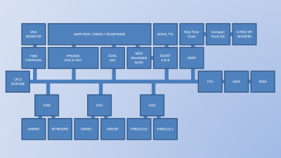
MARC-3 S Block diagram.png [ 116.13 KiB | Viewed 6859 times ]


For about 65% of the above mentioned devices / modules I have finished the schematics and PCB layouts, these include the CPU-, CPLD-, RAM-, ROM- and DUART-board. These will be stackable and the basic design for MARC-3 S.

I bought a bunch of 12-pin Arduino headers and 120 x 80 mm single sided copper clads: the build can begin!
Next I’m going to present the CPU-board.

_________________
Marco


Top
 Profile  
Reply with quote  
 Post subject: Re: MARC-3 S
PostPosted: Tue Jan 23, 2018 10:05 pm 
Offline
User avatar

Joined: Fri Dec 11, 2009 3:50 pm
Posts: 3346
Location: Ontario, Canada
Nice feature set! 8)

Something I'd be cautious about is the single-sided boards -- which generally are okay, but are NOT great where mechanical stress is present. I'm thinking about the headers you mentioned. These will probably be subjected to a fair amount of wiggling during the insertions and removals that can be expected.

Ideally what you want is for the header pins to be soldered into plate-through holes -- as with the Arduino. Unfortunately, foil only (ie: no plate-through) is much less robust. If plate-through holes are out of the question then at least consider using dual-row headers, not single-row, because the two rows buttress one another to some extent.

Great project! Have fun, and keep us posted!

-- Jeff

_________________
In 1988 my 65C02 got six new registers and 44 new full-speed instructions!
https://laughtonelectronics.com/Arcana/ ... mmary.html


Top
 Profile  
Reply with quote  
 Post subject: Re: MARC-3 S
PostPosted: Tue Jan 23, 2018 10:59 pm 
Offline

Joined: Wed Sep 11, 2013 8:43 pm
Posts: 207
Location: The Netherlands
Thanks!

I didn’t think of the mechanical stress. These special stackable pin headers come only in 12 x 1 or smaller, and I bought quite a few of them as I need six per board, and for the bare minimum computer I need five boards. So another option isn’t feasible. However, being aware of this, I can take some precautions, like lubricate them with contact spray before inserting them. I also could consider not inserting them all the way through, leaving one mm space. OTOH, I guess inserting them will push the copper onto the board, but pulling them out will probably put a lot more stress on the pads.

Yes, it’s an extensive feature set, I’ve fantasized and designed it for a long time, so I got carried away. :) Especially the F18A, FPGASID and the DreamBlaster X2 are very nice devices to play with. The FPGASID will be released very soon for the public and I have pre-ordered a long time ago.

However, although it’s a simplified version of my MARC-2 design, getting those first five boards: CPU, CPLD, RAM, ROM and DUART to work, is my first goal. Then I can add the goodies and stuff. :P

_________________
Marco


Top
 Profile  
Reply with quote  
 Post subject: Re: MARC-3 S
PostPosted: Wed Jan 24, 2018 4:42 am 
Offline

Joined: Sat Jun 04, 2016 10:22 pm
Posts: 483
Location: Australia
I would put the socket side of the stackable headers on the non-copper side, and make sure the connector was seated right up against the board, leaving very little room for movement.


Top
 Profile  
Reply with quote  
 Post subject: Re: MARC-3 S
PostPosted: Wed Jan 24, 2018 11:19 am 
Offline

Joined: Wed Sep 11, 2013 8:43 pm
Posts: 207
Location: The Netherlands
DerTrueForce wrote:
I would put the socket side of the stackable headers on the non-copper side, and make sure the connector was seated right up against the board, leaving very little room for movement.


Indeed, I think that would be best.

_________________
Marco


Top
 Profile  
Reply with quote  
 Post subject: Re: MARC-3 S
PostPosted: Wed Jan 24, 2018 11:32 am 
Offline

Joined: Wed Sep 11, 2013 8:43 pm
Posts: 207
Location: The Netherlands
The CPU board:
Attachment:
01-BUS-CPU05.sch.png
01-BUS-CPU05.sch.png [ 76.09 KiB | Viewed 6809 times ]


In the schematic you can see how the headers are organized by the physical layout of the CPU. Most boards won’t need more than a few jumper wires, so that they can be single sided.

I’ve treated the 65816 mystery pins according to this post and Garth’s primer.
However, from the several designs I’ve seen, they all treat them different.

VPB, ABORTB, MLB, E and MX will not (yet) be used. They are all outputs, except for ABORTB, which has a 3k3 pull-up. By means of a jumper, I could tie them to the headers, if needed. Otherwise I could use those header pins for other things, as a last resort if I’d run out of I/O pins on the CPLD.

[edit]
BE, NMIB, RDY, IRQB will initially be pulled high with a weak ‘1’ by the CPLD.
Actually, BE and RDY have external pull-ups.
NMIB and IRQB are set high while not in use.
[/edit]

Here’s the first PCB, simple and without jumper wires.
Attachment:
01-BUS-CPU05.brd.g.png
01-BUS-CPU05.brd.g.png [ 59.94 KiB | Viewed 6809 times ]


The filled copper polygon is connected to ground, I think that would improve performance?

_________________
Marco


Last edited by lordbubsy on Sat Jan 27, 2018 2:17 am, edited 1 time in total.

Top
 Profile  
Reply with quote  
 Post subject: Re: MARC-3 S
PostPosted: Fri Jan 26, 2018 8:19 pm 
Offline

Joined: Wed Sep 11, 2013 8:43 pm
Posts: 207
Location: The Netherlands
After over etching the first board, the second turned out fine.
Attachment:
CPU board back.jpg
CPU board back.jpg [ 1.04 MiB | Viewed 6753 times ]

Here's a virgin 65816! :P
Attachment:
CPU board front.jpg
CPU board front.jpg [ 1.08 MiB | Viewed 6753 times ]

_________________
Marco


Top
 Profile  
Reply with quote  
 Post subject: Re: MARC-3 S
PostPosted: Sat Jan 27, 2018 3:35 pm 
Offline

Joined: Wed Sep 11, 2013 8:43 pm
Posts: 207
Location: The Netherlands
The CPLD board:

Attachment:
02-CPLD07.sch.png
02-CPLD07.sch.png [ 113.73 KiB | Viewed 6727 times ]


As glue logic I’m going to use the XC9572 PLCC84 or the XC95108 PLCC84 if I need more resources. This board is also very straight forward, all I/O pins of the CPLD are connected to the headers, except for the 16MHz clock input, which will come from another source. There are 72 pins in total on the headers, 68 of them are I/O. Two pins are N.C. and the remaining two are +5V and GND. By the way, each board will be connected with a separate power connector, which will provide a more evenly power distribution. A de-bounced reset signal N_RESET, also coming from another source, is added to the headers.

This board is going to provide quite some tasks:
• System clock divider to provide a strong 50% duty cycle PHI2
• SPI External Clock generator
• Reset circuit
• Tri-state various pins during RESET
• UPPER address latch for the ‘816
• Memory read/write qualified with PHI2
• VDA VPA address qualification
• RAM chip selects
• I/O chip selects
• Set 65816 Inputs to defined states
• IRQ handler
• NMI handler

Attachment:
02-CPLD07.brd.c1.png
02-CPLD07.brd.c1.png [ 116.19 KiB | Viewed 6727 times ]

Attachment:
02-CPLD07.brd.g.png
02-CPLD07.brd.g.png [ 98.64 KiB | Viewed 6727 times ]

Attachment:
CPLD front.jpg
CPLD front.jpg [ 1.17 MiB | Viewed 6727 times ]

This board needs a few jumper wires for +5V and GND. I had to bring the JTAG connector to the side because of the tight space between the boards. I'll be ordering this kind of connecors.
Attachment:
WTBSTW.png
WTBSTW.png [ 91.57 KiB | Viewed 6727 times ]


I've tested the boards for shorts and open circuits, everything seems OK so far.
Next I'm going to test them with a slow clock seperately, and then together...

_________________
Marco


Top
 Profile  
Reply with quote  
 Post subject: Re: MARC-3 S
PostPosted: Wed Jan 31, 2018 2:19 pm 
Offline

Joined: Wed Sep 11, 2013 8:43 pm
Posts: 207
Location: The Netherlands
I’ve tested the CPU and CPLD board for shorts and open connections. I’ve also tested the CPU with a free run by setting the data bus to $EA using 10k Ohm resistors. I used a VERY slow clock of about 1 Hz and cranked it up to several kHz and watched the address lines behave like they should.

The clock that I use is an 555 timer astable circuit, eventually I had to add a 74HC74 to get a strong enough clock to make the circuits work perfectly stable. I find this variable slow clock very handy to test the circuit, at least now in the beginning.
Attachment:
Clock for free run test.png
Clock for free run test.png [ 43.23 KiB | Viewed 6687 times ]

For testing the CPLD board, I connected the clock to the first global CPLD clock input and tested all 68 I/O lines individually with a probe. I noticed that the CPLD is even more sensitive for getting a proper clock despite of setting the slew rate of all pins to slow.

;----

Now I stacked the two boards together and want to perform a free run using the CPLD.

According to the W65C816S datasheet, data can be read by the CPU when RWB is high and PHI2 is low, or is it just at a brief moment when PHI2 is on the falling edge?

So which VHDL code do I have use:

Code:
D  <= "11101010" when ((PHI2='0') and (RWB='1')) else
      "ZZZZZZZZ";


Or

Code:
process (PHI2)
   begin
      if (falling_edge(PHI2) and (RWB='1')) then
      D  <= "11101010" else
            "ZZZZZZZZ";
end process;

The complete code for this test looks like:
Code:
library IEEE;
use IEEE.STD_LOGIC_1164.ALL;
use IEEE.STD_LOGIC_ARITH.ALL;
use IEEE.STD_LOGIC_UNSIGNED.ALL;

entity MARC3SVb is
    Port (
           CLOCK : in  STD_LOGIC;
           N_RESET : in  STD_LOGIC;
           D : inout  STD_LOGIC_VECTOR (7 downto 0);
           IRQB : out  STD_LOGIC;
           NMIB : out  STD_LOGIC;
           PHI2 : inout  STD_LOGIC;
           RWB : in  STD_LOGIC;
           RESB : out  STD_LOGIC);

end MARC3SVb;

architecture Behavioral of MARC3SVb is

signal CDIV        : std_logic_vector(4 downto 0);      --System clock divider

begin

process (CLOCK)
--System clock generator / divider
--Uses 1 to 5 registers depending on the counter width needed
   begin
      if (rising_edge(CLOCK)) then
         CDIV <= CDIV + '1';             --Increment DIV at CLOCK rate 16MHz
      end if;
PHI2 <= CDIV(0);                                        --Choose the desired CDIV(x) for speed
                                                        --CDIV(4) = PHI2 = CLOCK /  32 = 500kHz
                                                        --CDIV(3) = PHI2 = CLOCK /  16 = 1MHz
                                                        --CDIV(2) = PHI2 = CLOCK /   8 = 2MHz
                                                        --CDIV(1) = PHI2 = CLOCK /   4 = 4MHz
                                                        --CDIV(0) = PHI2 = CLOCK /   2 = 8MHz
end process;

--CPU data bus READ control, fixed to $EA = %11101010 NOP
--data that moves to CPU data bus, i.e. the CPU reads
--in all other cases, the D bus is tri-stated

process (PHI2)
   begin
      if (falling_edge(PHI2) and (RWB='1')) then
      D  <= "11101010" else
            "ZZZZZZZZ";
end process;

--Set 65816 Inputs to defined states
IRQB       <= '1';                                      --IRQ is not in use yet
NMIB       <= '1';                                      --NMI is not in use yet

end Behavioral;

_________________
Marco


Top
 Profile  
Reply with quote  
 Post subject: Re: MARC-3 S
PostPosted: Wed Jan 31, 2018 3:31 pm 
Offline
User avatar

Joined: Fri Dec 11, 2009 3:50 pm
Posts: 3346
Location: Ontario, Canada
lordbubsy wrote:
So which VHDL code do I have use:

Code:
D  <= "11101010" when ((PHI2='0') and (RWB='1')) else
      "ZZZZZZZZ";
You need to change PHI2='0' to PHI2='1', but otherwise this looks as if it might be OK. (I'm certainly not a VHDL expert.) Anyway, what you're doing is pretending to be memory, and during a read cycle the CPU expects memory to drive the data bus during the entire time Phi2 is high. Then when Phi2 falls the CPU latches what's already been placed on the bus -- and that's when memory can stop driving the bus. But it starts doing so when Phi2 goes high.

lordbubsy wrote:
I noticed that the CPLD is even more sensitive for getting a proper clock despite of setting the slew rate of all pins to slow.
Yeah, the clock input is gonna be sensitive -- especially with fast, modern chips. As for the slew rate setting, that determines how the outputs of the CPLD respond. Best to leave 'em slow unless you're sure there's a good reason to do otherwise.

Hope this helps!

_________________
In 1988 my 65C02 got six new registers and 44 new full-speed instructions!
https://laughtonelectronics.com/Arcana/ ... mmary.html


Top
 Profile  
Reply with quote  
 Post subject: Re: MARC-3 S
PostPosted: Wed Jan 31, 2018 3:43 pm 
Offline

Joined: Wed Sep 11, 2013 8:43 pm
Posts: 207
Location: The Netherlands
Thanks!
So it's not a clocked event. I'll try with PHI2='1'.

_________________
Marco


Top
 Profile  
Reply with quote  
 Post subject: Re: MARC-3 S
PostPosted: Wed Jan 31, 2018 4:45 pm 
Offline
User avatar

Joined: Fri Dec 11, 2009 3:50 pm
Posts: 3346
Location: Ontario, Canada
lordbubsy wrote:
it's not a clocked event.
Right, because you're doing a read, and in that context the CPLD is transmitting to the CPU (which receives). IOW memory (or your CPLD) places data on the bus and leaves it there. After things've had a moment to settle down, the CPU latches or clocks the data in, and the cycle is complete.

During a write cycle it's the CPU which places data on the bus and leaves it there -- and, after things've had a moment to settle down, memory (or your CPLD or whatever) latches or clocks the data in.

(In both cases it's usually the rise of Phi2 that cues the transmitting device to begin driving the bus -- only because that's a simple and convenient arrangement. But for this function there's nothing special about the rise of Phi2 -- IOW a different (later) timing signal could cue the data bus to be driven. Later is OK, as long as you provide that moment to settle down before Phi2 goes low (listed as the setup time in the specs)).

(This andother timing topics are covered in my Visual Guide to 65xx CPU Timing )

_________________
In 1988 my 65C02 got six new registers and 44 new full-speed instructions!
https://laughtonelectronics.com/Arcana/ ... mmary.html


Top
 Profile  
Reply with quote  
 Post subject: Re: MARC-3 S
PostPosted: Wed Jan 31, 2018 7:57 pm 
Offline

Joined: Wed Sep 11, 2013 8:43 pm
Posts: 207
Location: The Netherlands
That explains it all! Your diagrams are MUCH clearer than the WDC’s datasheet to me. I did see your timing diagrams on the forum before, but not the explanation on your website.

So here is the perfectly working free run “NOP loop” VHDL code for the W65C816S:

Code:
library IEEE;
use IEEE.STD_LOGIC_1164.ALL;
use IEEE.STD_LOGIC_ARITH.ALL;
use IEEE.STD_LOGIC_UNSIGNED.ALL;

entity MARC3SVb is
    Port (
           CLOCK : in  STD_LOGIC;
           D : inout  STD_LOGIC_VECTOR (7 downto 0);
           IRQB : out  STD_LOGIC;
           NMIB : out  STD_LOGIC;
           PHI2 : inout  STD_LOGIC;
           RESB : out  STD_LOGIC;
           RWB : in  STD_LOGIC);

end MARC3SVb;

architecture Behavioral of MARC3SVb is

signal CDIV        : std_logic_vector(4 downto 0);      --System clock divider

begin

process (CLOCK, CDIV)
--System clock generator / divider
--Uses 1 to 5 registers depending on the counter width needed
   begin
      if (rising_edge(CLOCK)) then
         CDIV <= CDIV + '1';             --Increment DIV at CLOCK rate 16MHz
      end if;
PHI2 <= CDIV(0);                                        --Choose the desired CDIV(x) for speed
                                                        --CDIV(4) = PHI2 = CLOCK /  32 = 500kHz
                                                        --CDIV(3) = PHI2 = CLOCK /  16 = 1MHz
                                                        --CDIV(2) = PHI2 = CLOCK /   8 = 2MHz
                                                        --CDIV(1) = PHI2 = CLOCK /   4 = 4MHz
                                                        --CDIV(0) = PHI2 = CLOCK /   2 = 8MHz
end process;

--CPU data bus READ control, fixed to $EA = %11101010 NOP
--data that moves to CPU data bus, i.e. the CPU reads
--in all other cases, the D bus is tri-stated
D  <= "11101010" when ((PHI2='1') and (RWB='1')) else
      "ZZZZZZZZ";

--Set 65816 Inputs to defined states
IRQB       <= '1';                                      --IRQ is not in use yet
NMIB       <= '1';                                      --NMI is not in use yet
RESB       <= '1';

end Behavioral;


I can observe that the data lines are set / reset when PHI2 is high, and the address lines are increasing each two PHI2 cycles.

Great, next I’m going to build the RAM board.

_________________
Marco


Top
 Profile  
Reply with quote  
 Post subject: Re: MARC-3 S
PostPosted: Sun Feb 11, 2018 6:36 pm 
Offline

Joined: Wed Sep 11, 2013 8:43 pm
Posts: 207
Location: The Netherlands
The RAM board has two stacks of two 512KiB SRAM’s, making a total of 2MiB.
Attachment:
03-RAM03.sch.png
03-RAM03.sch.png [ 73.38 KiB | Viewed 6602 times ]

Attachment:
RAM board front.jpg
RAM board front.jpg [ 971.27 KiB | Viewed 6602 times ]

RAM and EPROM chip select are working fine. Because I have no I/O devices connected to my computer at all, I used a program to test ROM and RAM functionality by checking the address lines going low and high.

Code:
; ROM test
; at 1 mhz, the address lines toggle at about 2 second intervals
; program counter will jump from to
; $c000 = %1100 0000 0000 0000
; $ff00 = %1111 1111 0000 0000
; check A8, A9, A10, A11, A12 and A13 for toggling
*   =   $c000
start1      lda #$6
loop0      ldy #$ff
loop1      ldx #$ff
loop2      dex
      bne loop2
      dey
      bne loop1
      sec
      sbc #1
      bne loop0
      jmp start2

*   =   $ff00
start2      lda #$6
loop3      ldy #$ff
loop4      ldx #$ff
loop5      dex
      bne loop5
      dey
      bne loop4
      sec
      sbc #1
      bne loop3
      jmp start1

*   =   $fffa
!word      $d000      ; nmi vector
!word      $c000      ; reset vector
!word      $d000      ; irq vector


Code:
; RAM test
; at 1 mhz, the address lines toggle at about 2 second intervals
; program counter will jump from to
; $c000 = %1100 0000 0000 0000
; $1000 = %0001 0000 0000 0000
; check A12, A14 and A15 for toggling
*   =   $c000
init      ldx #0
-      lda start2,x
      beq start1
      sta $1000,x
      inx
      bne -

start1      lda #$6
loop0      ldy #$ff
loop1      ldx #$ff
loop2      dex
      bne loop2
      dey
      bne loop1
      sec
      sbc #1
      bne loop0
      jmp $1000


start2      lda #$6
loop3      ldy #$ff
loop4      ldx #$ff
loop5      dex
      bne loop5
      dey
      bne loop4
      sec
      sbc #1
      bne loop3
      jmp start1
      !byte 0

*   =   $fffa
!word      $d000      ; nmi vector
!word      $c000      ; reset vector
!word      $d000      ; irq vector

Attachment:
post05 RAM EPROM.jpg
post05 RAM EPROM.jpg [ 1.6 MiB | Viewed 6602 times ]


At the far end on the bread board there are an ATmega1284P and two 74HC595’s. These are for the ROM emulator, clock and reset. I have prototyped them and the ROM board is in the making.
I guess it's not really a ROM emulator, but more like a RAM programmer. :)

_________________
Marco


Top
 Profile  
Reply with quote  
 Post subject: Re: MARC-3 S
PostPosted: Sun Feb 25, 2018 4:33 pm 
Offline

Joined: Wed Sep 11, 2013 8:43 pm
Posts: 207
Location: The Netherlands
Finally, I’ve got a working system!
Attachment:
working CPU CPLD RAM EEPROM.jpg
working CPU CPLD RAM EEPROM.jpg [ 1.36 MiB | Viewed 6510 times ]

The fourth board became a “simple” EEPROM AT28C256 board.
I only decoded it to 0C000-0FFFF.

The CPLD logic does not yet:
• Decodes addresses A16..A18, they are just set to “000”
• Decodes the four SRAM chip selects, they are just set to “1110”
• Do anything with IRQ or NMI, they are both set to “1”
So that’s something to do, but it’s working so far.

I plan on copying the EEPROM’s contents to RAM during RESET and turn the it off for more speed. The AT28C256 is only 150ns, so that should be good for 6,67 MHz, but the contraption above actually runs at 8 MHz, however that’s without any I/O devices.

Besides the EEPROM I also have two of these puppy’s lying around:
Attachment:
EPROMS.jpg
EPROMS.jpg [ 594.25 KiB | Viewed 6510 times ]

They are 2MiB, 100ns, that’s good for 10 MHz. I could use them for permanent math tables, graphics or sound samples etc. I don’t expect my computer to run at more than a maximum of 8 to 10 MHz.

I’m not planning to implement DMA or a co-processor because at a max of 8 to 10 MHz and the 24 bit address and 16 bit data capabilities of the 65816, I don’t really need that. I do plan my software to run in a 60Hz interrupt loop, that is, the F18A is generating a VBLANC signal. That means that graphic updates are performed at each new frame. In those 16,66ms, the CPU can do a lot more things than a C64 for instance.

So finally substantial progress! Next I’m going to implement the DUART.

_________________
Marco


Top
 Profile  
Reply with quote  
Display posts from previous:  Sort by  
Post new topic Reply to topic  [ 23 posts ]  Go to page 1, 2  Next

All times are UTC


Who is online

Users browsing this forum: No registered users and 5 guests


You cannot post new topics in this forum
You cannot reply to topics in this forum
You cannot edit your posts in this forum
You cannot delete your posts in this forum
You cannot post attachments in this forum

Search for:
Jump to: