6502.org Forum  Projects  Code  Documents  Tools  Forum
It is currently Sat Apr 27, 2024 4:41 pm

All times are UTC


Post new topic Reply to topic  [ 25 posts ]  Go to page 1, 2  Next
Author Message
PostPosted: Sun Dec 24, 2023 2:50 am 
Offline

Joined: Fri Jul 09, 2021 10:12 pm
Posts: 741
This is not strictly a 6502 circuit, though it is designed to work with my 6502 computers - however I thought it might be of interest anyway, and I apologise if it's off-topic or otherwise not interesting.

As I mentioned in another thread, I wanted some basic VGA output for one of my computers, and wanted to build something much simpler than my past video circuits which have all been graphical. This is what I came up with, using some GAL SPLDs (ATF16V8) to reduce the chip count:
Attachment:
vgatextschematic.png
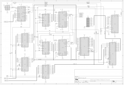
vgatextschematic.png [ 114.52 KiB | Viewed 1881 times ]

The circuit has three ATF16V8 PLDs, two 74HCT590 8-bit tristate counters, three 74AHC574 8-bit tristate registers, a 71256-SA12 32K SRAM module of which 4K gets used, an AT28C256 32K EEPROM module of which 4K gets used, a 74HCT166 parallel-in serial-out shift register, and the VGA oscillator (25.175MHz). It fits on two rows of breadboard:
Attachment:
20231223_133909.jpg
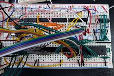
20231223_133909.jpg [ 698.9 KiB | Viewed 1879 times ]

It is black and white only, with no support for character attributes, but I may add this later. The font is one of the standard VGA fonts, 8x16, in a 640x480 resolution mode - this existed on PCs but was not so common, they usually used 9x16 characters in a 720x400 resolution mode instead. So we get 80x30 characters on the screen:
Attachment:
20231222_061117.jpg
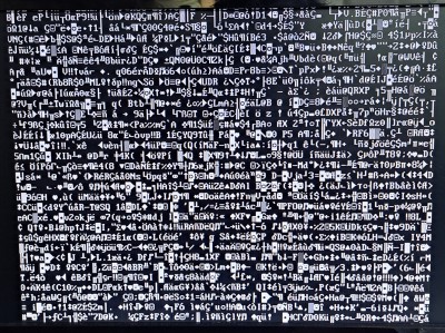
20231222_061117.jpg [ 1.23 MiB | Viewed 1879 times ]

Regarding its operation, I'm not sure how much detail to go into, but I'll write what comes to mind and do ask if anything is unclear.

At a high level it reads a byte from RAM once per eight VGA pixels, and shifts it out through the shift register. Hence it does this at an eighth of the pixel clock frequency, which is about 3MHz. The RAM is plenty fast enough to do write operations in between these reads, when they are necessary. Unlike my previous circuits, this one is not tied no the same clock as the CPU - I let them run on separate clocks. Any writes from the CPU are captured in storage registers, forming a 1-deep FIFO, and processed by the video circuit when the time is right. It's up to the software code to not write more frequently than the circuit can support, but this would actually be quite hard to do with a 6502, you'd need a very fast clock speed and a very simple data stream.

The "control" PLD controls the timing signals for the various components, within each block of eight horizontal pixels - it tells the counters and RAM when they can output to the buses, tells the shift register when it should load the next 8 bits of data, and watches out for writes from the computer and, if one is pending, it arranges for the storage registers to output to the buses instead of the counters, and sends the RAM a write-enable pulse at the right time.

The "horizontal" and "vertical" PLDs work in tandem with one of the counters each, to generate the sync signals for the monitor, as well as the reset signals for the counters and an "on" signal which shows when the monitor is not in a blanking period, hence we should output visible pixel data.

In more detail, here's the code for the control PLD:
Code:
Name     vgatextctl ;
PartNo   17.00.A ;
Date     21/12/2023 ;
Revision 00 ;
Designer George Foot ;
Company  gfoot360 ;
Assembly None ;
Location None ;
Device   g16v8 ;

pin 1 = CLK;

/* inputs */
pin 2 = CLK1;
pin 3 = !WR;
pin [4..8] = [ ENA4..1, !ENA0 ];

/* outputs */
pin 12 = C0;      /* clk/2, HCPR */
pin 13 = C1;      /* clk/4 */
pin 14 = C2;      /* clk/8, HCPC, /COE */
pin 15 = !XOE;    /* OE for write ops */
pin 16 = !RAMWE;  /* RAM's /WE */
pin 17 = !SRPE;   /* shift reg parallel enable */
pin 18 = WP;      /* write pending */
pin 19 = PREVWR;  /* WR from previous cycle */

nC0 = !C0;
nC1 = C0 & !C1 # !C0 & C1;
nC2 = C0 & C1 & !C2 # !C0 & C2 # !C1 & C2;

Field C = [ C2..0 ];
Field nC = [ nC2..0 ];
C.d = nC;

XOE.d = WP & nC:5 # XOE & nC:[4..7];
RAMWE.d = XOE & nC:6;

SRPE = !CLK1 & C:2 # CLK1 & C:3;

Field ENA = [ENA4..0];
PREVWR.d = WR & ENA:&;
WP.d = WP & !(C:7 & XOE) # PREVWR & !WR;
The control PLD counts up from 0 to 7, based on the VGA pixel clock, using macrocells C0,C1,C2 - grouped together as field C. The temporary field nC is used to track the "next" value for C, as it can be useful to reuse this in other registered pin calculations as often their states need to correspond to the next value, rather than the current value. This is just a nicety in the source file though, it doesn't use any hardware resources.

The high bit of this count, C2, forms a "counter output enable" signal (COE) which allows the counters - and RAM - to output their data. Thus the counters drive the V and H buses, the and RAM looks up the data there and outputs it to the video data (VD) bus. The ROM picks this up along with the bottom four bits of the V bus to look up a row of data from the relevant character definition, and provides this to the shift register. The shift register's parallel-enable pin SRPE is pulled low for one tick out of every eight, by the control PLD. Originally this was at the end of COE's low phase, but I moved it back a tick or two due to artifacts appearing. SRPE is not registered because it needs to straddle a rising edge of the pixel clock - I want to set it halfway through a clock period, and clear it halfway through the next one.

During write operations, the control PLD spots that a write is occuring based on the input WE signal being asserted along with all five enable inputs being asserted. This state is latched until the eight-pixel cycle gets to a point where the write can take place. When this is reached, the storage registers' output-enable (XOE) is activated by the control PLD, so that they write to the video address and data buses. It used to do this immediately after COE was unasserted, but I changed it to leave a one clock gap with nothing driving the buses. One clock cycle later, the control PLD activates the RAM's write-enable signal for a further clock cycle, and then the "write pending" signal is cleared. This activation of XOE and RAMWE only happens during cycles where there is data to be written.

To illustrate how the timing for reads and writes work together, here is the simulator script to test the PLD:
Code:
ORDER: CLK, CLK1, %1, WR, %1, ENA, %2, C, %1, PREVWR, WP, %2, XOE, RAMWE, %1, SRPE;

VECTORS:

$msg "Read";
P0 0 11111  '0' 0 0  11 0
00 0 11111  "0" L L  LL L
C1 0 11111  "1" L L  LL L
C1 0 11111  "2" L L  LL L
00 0 11111  "2" L L  LL H
C1 0 11111  "3" L L  LL H
00 0 11111  "3" L L  LL L
C1 0 11111  "4" L L  LL L
C1 0 11111  "5" L L  LL L
C1 0 11111  "6" L L  LL L
C1 0 11111  "7" L L  LL L
C1 0 11111  "0" L L  LL L

$msg "Write";
C1 1 11111  "1" H L  LL L
C1 0 11111  "2" L H  LL L
00 0 11111  "2" L H  LL H
C1 0 11111  "3" L H  LL H
00 0 11111  "3" L H  LL L
C1 0 11111  "4" L H  LL L
C1 0 11111  "5" L H  HL L
C1 0 11111  "6" L H  HH L
C1 0 11111  "7" L H  HL L
C1 0 11111  "0" L L  LL L


Moving on to the horizontal PLD:
Code:
Name     vgatexthoriz ;
PartNo   17.00.B ;
Date     21/12/2023 ;
RevisiON 00 ;
Designer George Foot ;
Company  gfoot360 ;
Assembly None ;
LocatiON None ;
Device   g16v8 ;

pin 1 = CLK; /* C2 */

/* 74HCT590 8-bit counter, CPR=C2, CPC=!C2, MRC=!HR */
pin [2..8] = [H0..6];
pin 9 = VON;
/* 0 spare inputs */

pin 17 = !HR;
pin 18 = !ON;
pin 19 = !HSYNC;
/* 5 spare I/Os */

Field H = [H6..0];

HR.d = H:62;
ON.d = H:63 & VON # ON & !(H:4f);
HSYNC.d = H:51 # HSYNC & !(H:5d);
It is fairly straightforward - the external counter is providing a 7-bit count value, and based on various values for this count, we do different things. The 74HC590s have asynchronous reset, which is annoying; but they also have separate clock pins for counting and outputting the latest count. The async reset means we don't want the counter to be clocked at the same point as the PLD, because then we'd be transitioning the MR input to the counter at the same point that it's being clocked. So we drive the PLD from a different signal that's in sync with the counter's register clock instead. This means that outputs from the PLD and the counter change at roughly the same time. The counter internally counts up to the next value in the meantime but the outside world - including the PLD - doesn't see that until the CPR tick.

The upshot of this is that we want the counter to be internally, asynchronously reset when it has just published the final count value for the row, which is 99 ($63) for us. To do this, the PLD needs to make the decision to assert VR - the reset signal - when the published count is one less than that, i.e. $62. This was confusing to think about but made sense in the end.

The trigger value for the ON signal is, however, $63 because we want this to be activated on the cycle when the counter starts outputting zero - so we want to set it in the transition from the cycle where the counter was outputting $63, which is also the cycle when it will be reset (I could have used that instead of a specific value here). ON gets turned off when the horizontal count is about to tick over to 80 characters ($50) so the trigger value for that is $4F.

The trigger values for HSYNC are similarly one less than you might expect - they are the values the counter will show on the cycle before HSYNC should start or end.

The vertical PLD is similar to the horizontal one, but has to deal with much larger count values:
Code:
Name     vgatextvert;
PartNo   17.00.C ;
Date     21/12/2023 ;
Revision 01 ;
Designer George Foot ;
Company  gfoot360 ;
Assembly None ;
Location None ;
Device   g16v8 ;

pin 1 = CLK; /* hsync */

/* 74HCT590 8-bit counter, e.g. CPR=hsync, CPC=!hsync, /MRC=!vr */
pin [2..9] = [V0..7];
/* 0 spare inputs */

pin 12 = !VR;
pin 13 = !VSYNC;
pin 14 = VON;
pin 15 = V8int;
pin 16 = V8;
pin 17 = !V8OE;

/* 2 spare I/Os */

Field V = [V7..0];

VR.d = V8int & V:de # !VON & V:2b;
!VON.d = VON & V8int & V:df # !VON & !(V:[2c..2f]);
V8int.d = VON & (V:ff # V8int);
VSYNC.d = !VON & V:[09..0a];

V8 = V8int;
V8.oe = V8OE;
There are 525 scanlines on the screen, but the counter can only count up to 255 before wrapping. To count up to 525, it needs to go through three phases:
  • Phase 1 - scanlines 0-255 - VON is set, V8int is unset; but is set at the very end of this phase
  • Phase 2 - scanlines 256-479 - VON is set, V8int is set; we count up to 223 and then reset the counter
  • Phase 3 - scanlines 480-524 - VON is not set as this is the blanking period; we count up to 45 then reset the counter, also generating VSYNC in the right place
VON is output for the horziontal PLD to read, and blend with its own blanking signal. The blanking is done by disabling the character ROM, whose data bus has pull-down resistors, so the shift register outputs black from that point on.

V8int is for internal use, but we also need this signal externally. However it needs to be tristate as it's going on to the video address bus which is sometimes driven by the write circuit instead. This PLD doesn't allow us to individually set output-enable for a registered pin; however, it does allow us to do it for a combinational pin. So we copy the state from V8int into V8, and set that pin up to be controllable by an external signal.

We can't use the PLD's general output-enable pin for this purpose because there are other output signals on this PLD such as VSYNC which must be active all the time, not just during the read portion of each 8-pixel cycle.

---

Talking of output-enables, an important factor in this circuit is that the outputs from the 74HC590s are used to determine the next states for the PLDs, but these outputs are also not always enabled - they are only enabled when COE is low. This means that it's important for the horizontal and vertical PLDs' clock inputs to have their rising edges during that period. For the horizontal one that's straightforward enough, but for the vertical one it's less obvious because its clock signal comes from the horizontal one. As the horizontal one is clocked by the end of the COE signal, this means COE is not asserted when the vertical one is clocked. However I delayed the XOE signal by one clock tick so that, at this point, the bus would at least float, which is sufficient. I ought to go back and find a better way to do that really.

There is also a bug, it seems, with write operations where sometimes - maybe one it a hundred - they don't go through, or perhaps write the wrong data. I don't think they are writing the wrong addresses. It appears mostly worked-around by making the software execute write operations twice, which I guess reduces the chance to one in ten thousand that it fails! I haven't worked out what actually causes it yet though, there are several places it could be going wrong en route from the computer to the video RAM, and if the problem persists then I will look into it more.

You can also tell how much trouble I had with a circuit by how many passive components it has in it. There are quite a few decoupling capacitors in this one, and there's even one straddling across the shift register. This is because the shift register was giving me a lot of problems. I think this one is actually broken because if I connect its pin 1 (serial input) high then it seems to bleed this into the other data, even though it should be getting loaded before this value has time to propagate to the output; similarly if I connect it low, everything goes black. It is an input so I didn't want to leave it unconnected, and I found that connecting it high through a large resistor seemed to work.

I also had trouble with the clock edges, even though it is physically right next to the oscillator. I added parallel termination to the clock line at the shift register's clock input pin - I think this is 220 ohms, it is a value I've used before for this exact same purpose and it fixed a lot of flickering and sparkling around the text.

At some point I would like to add colour support, and perhaps get rid of the ROM and let the font definition live in RAM with the framebuffer. I have a scheme in mind to hit the RAM four times during the eight pixel cycle, to do this - once to read the attribute byte, once to read the character index, once to read the line of pixels to from the character, and potentially a fourth time to write new data into RAM. This would involve three different possible sources for address data for the RAM, rather than just two, but I think it should be fairly practical to achieve and maybe a cleaner solution than having a separate RAM IC for storing attribute data.

I also thought about some kind of hybrid text and graphics support, but haven't fleshed that idea out properly yet - I'd only want to do it if it can be done without too much complexity.

In any case it looks like the circuit as it stands should satisfy my immediate needs, so I don't know if/when I'd come back and make those changes.


Top
 Profile  
Reply with quote  
PostPosted: Sun Dec 24, 2023 4:15 am 
Offline

Joined: Fri Dec 21, 2018 1:05 am
Posts: 1076
Location: Albuquerque NM USA
Great work. Having done a CPLD version like this I can appreciate it is more challenging to divide the video generation function into 3 SPLD. It is probably twice as hard to explain! The detailed timings and race condition must be quite challenging. Dual port RAM can simplify with integration of text, attribute, and font in one memory device. Are you able to write anytime without the "snow" effect?
Bill


Top
 Profile  
Reply with quote  
PostPosted: Sun Dec 24, 2023 11:11 am 
Offline

Joined: Fri Jul 09, 2021 10:12 pm
Posts: 741
This was in the other thread but I'll answer here to keep the video-related stuff together:
barnacle wrote:
I'm at the stage of working out the character set for my half-svga display: would you care to share your character rom?
https://int10h.org/oldschool-pc-fonts/fontlist/ is a great way to browse a variety of old PC fonts. They are available for download but it seems not in bitmapped format. So I got the actual font from https://github.com/viler-int10h/vga-tex ... 2FVGA8.F16 which has a similar amount of fonts, in raw bitmap format, but isn't as easy to browse.

I just burned this exact file into my EEPROM, the format was exactly what I needed.


Top
 Profile  
Reply with quote  
PostPosted: Sun Dec 24, 2023 11:35 am 
Offline

Joined: Fri Jul 09, 2021 10:12 pm
Posts: 741
plasmo wrote:
Great work. Having done a CPLD version like this I can appreciate it is more challenging to divide the video generation function into 3 SPLD. It is probably twice as hard to explain!
Yes I'm never sure how much detail to give! But I know there are a lot of people around experimenting with these chips who might like to see the code, so went into some detail there.

The split wasn't too hard because really the functions are quite separate and independent. One of the key factors is which clock signal a set of outputs needs to change on. These devices require all registered outputs to change on the same clock. However, I do think I could probably have moved the first vertical bits into the horizontal PLD and saved some complexity from that. It would then work well for graphics too, with double scanning still done by the character row count.

Quote:
The detailed timings and race condition must be quite challenging. Dual port RAM can simplify with integration of text, attribute, and font in one memory device. Are you able to write anytime without the "snow" effect?
No there's no snow, the writes are cleanly out of the way. When I was activating XOE from C counts 4-7, exactly opposite to COE, it was causing loss of sync, due I believe to the fact that the vertical PLD is clocked during C=4 and XOE was already active at that point, overwriting the bus with the write registers. And I originally had the SRPE signal spanning the clock pulse between C=3 and C=4 but that caused shimmering and sparkling in the text, so the shift register must have some hold time requirement there. These are the two things I fixed regarding image quality.


Top
 Profile  
Reply with quote  
PostPosted: Sun Dec 24, 2023 1:16 pm 
Offline

Joined: Mon Jan 19, 2004 12:49 pm
Posts: 660
Location: Potsdam, DE
gfoot wrote:
So I got the actual font from https://github.com/viler-int10h/vga-tex ... 2FVGA8.F16 which has a similar amount of fonts, in raw bitmap format, but isn't as easy to browse.


Thank you - I need 0x20 to 0x7f, no space by default for other characters at present; characters are in system ram, not an eprom. https://github.com/viler-int10h/vga-tex ... I8.F16.png looks handy for a first attempt: I have a character cell 8 bits wide (so seven available in most cases, absent kerning) and either 12 or 15 deep (for 25 or 20 character lines in 300 lines).

Neil


Top
 Profile  
Reply with quote  
PostPosted: Sun Dec 24, 2023 10:14 pm 
Offline
User avatar

Joined: Thu May 28, 2009 9:46 pm
Posts: 8144
Location: Midwestern USA
gfoot wrote:
This is not strictly a 6502 circuit...

TL:DR...

Lotta parts.  Why not use a single CPLD instead of multiple GALs?

_________________
x86?  We ain't got no x86.  We don't NEED no stinking x86!


Top
 Profile  
Reply with quote  
PostPosted: Sun Dec 24, 2023 11:08 pm 
Offline

Joined: Fri Jul 09, 2021 10:12 pm
Posts: 741
BigDumbDinosaur wrote:
Lotta parts. Why not use a single CPLD instead of multiple GALs?
It might be interesting one day, but at the moment I prefer sticking to parts that are readily available in DIP packages. I find that working within even arbitrary constraints like that is a nice challenge; and everyone has to draw a line somewhere otherwise we'd all just be making everything in verilog, or simulators - which is fine if you like that sort of thing, but seems too close to my day job for a hobby, for me!


Top
 Profile  
Reply with quote  
PostPosted: Tue Dec 26, 2023 12:47 am 
Offline

Joined: Sat Oct 28, 2023 7:57 pm
Posts: 15
Location: Missouri
gfoot wrote:
BigDumbDinosaur wrote:
Lotta parts. Why not use a single CPLD instead of multiple GALs?
It might be interesting one day, but at the moment I prefer sticking to parts that are readily available in DIP packages. I find that working within even arbitrary constraints like that is a nice challenge; and everyone has to draw a line somewhere otherwise we'd all just be making everything in verilog, or simulators - which is fine if you like that sort of thing, but seems too close to my day job for a hobby, for me!


I get that! I'm hoping to eventually use programmable logic to consolidate some things, but I enjoy the challenge doing that later. What do you use to program those chips (software wise)? With all the consolidation in the market it seems like I'm not sure which editor to download and ensure compatibility. Since I've been looking at GALs like yours, I figured I'd ask.


Top
 Profile  
Reply with quote  
PostPosted: Tue Dec 26, 2023 1:36 pm 
Offline

Joined: Fri Jul 09, 2021 10:12 pm
Posts: 741
WCMiller wrote:
What do you use to program those chips (software wise)? With all the consolidation in the market it seems like I'm not sure which editor to download and ensure compatibility. Since I've been looking at GALs like yours, I figured I'd ask.
I don't know about general advice as I haven't experimented with different options, but I use WinCupl. However, the user interface is terrible - very buggy, lots of crashes, and just bad design choices too - so I don't use that, I edit my code in a text editor just like any other code, and build it using the command line "cupl" tool that is part of WinCupl. To do that I use a wrapper script that sets some environment variables and also massages the output a bit. I also run it through Wine, on a Linux system, but of course it works under Windows too as that's what it was designed for.


Top
 Profile  
Reply with quote  
PostPosted: Tue Dec 26, 2023 2:16 pm 
Offline
User avatar

Joined: Wed Feb 14, 2018 2:33 pm
Posts: 1398
Location: Scotland
gfoot wrote:
WCMiller wrote:
What do you use to program those chips (software wise)? With all the consolidation in the market it seems like I'm not sure which editor to download and ensure compatibility. Since I've been looking at GALs like yours, I figured I'd ask.
I don't know about general advice as I haven't experimented with different options, but I use WinCupl. However, the user interface is terrible - very buggy, lots of crashes, and just bad design choices too - so I don't use that, I edit my code in a text editor just like any other code, and build it using the command line "cupl" tool that is part of WinCupl. To do that I use a wrapper script that sets some environment variables and also massages the output a bit. I also run it through Wine, on a Linux system, but of course it works under Windows too as that's what it was designed for.


The only other option that I'm aware of - which I use - is GALasm under Linux. From what I've seen, I don't think it's as flexible as CUPL but it seems to work for what I've used it for. My gripes is that it doesn't support ()'s in expressions so working stuff out is harder (for me, at least) than if I could just use ()'s and let the compiler sort it out... I have looked at CUPL under Wine, but it seems to only run under 32-bit mode and I was somewhat overwhelmed at the sheer number of packages it was going to pull in to make it work on my 64bit Linux desktop...

(And the actual programming part - I'm using old Lattice GALs and running the G540 programmer under an old Win XP Laptop - I need to upgrade my Linux minipro hardware to the TL866II Plus to do them as well as the Atmel/Microchip GALs under Linux)

-Gordon

_________________
--
Gordon Henderson.
See my Ruby 6502 and 65816 SBC projects here: https://projects.drogon.net/ruby/


Top
 Profile  
Reply with quote  
PostPosted: Tue Dec 26, 2023 4:18 pm 
Offline

Joined: Sat Oct 09, 2021 11:21 am
Posts: 703
Location: Texas
Very good looking George!

gfoot wrote:
V8int is for internal use, but we also need this signal externally. However it needs to be tristate as it's going on to the video address bus which is sometimes driven by the write circuit instead. This PLD doesn't allow us to individually set output-enable for a registered pin; however, it does allow us to do it for a combinational pin. So we copy the state from V8int into V8, and set that pin up to be controllable by an external signal.


Ah, that is brilliant :) Very good idea which I should keep in my back pocket if I need to do something similar.

Quote:
You can also tell how much trouble I had with a circuit by how many passive components it has in it.


I guess that's what breadboards are good for, testing things like that out. I remember back a long while ago, I had a 'canary' 74HC161 which would cause a lot of snow at room temperature or below. I swapped it for another '161 and it worked fine at room temperature. Jeff told me to not toss it, but try different timing signals, and sure enough it was MY fault, not the chip's! I still have my canary chip somewhere, separated, in case I want to test marginal timing issues again.

I'm telling this story to say to check for 'logic' problems, not necessarily 'chip' problems. I personally use so so few passives that when I see y'all talking about it I'm scared to think mine are working only by a fluke! But who knows.

That aside, I have done something similar in the past to what you are doing. (here https://github.com/stevenchadburrow/SerialVGA) My version is serial and not parallel like yours, but I suppose I could change out my '595s for '273s or something and have it parallel. I use the same clock speed as you, same size in RAM, same everything. What I do differently is putting those sync signals into a ROM instead of the GALs. This reduces chip count a LOT, where I think I only have 2 logic chips (besides all the requisite counters, latches, and shift registers). But to each their own!

Overall, I think separating the video clock from the CPU clock is a good way forward. Like you said, you can adjust write speed/frequency in software, and if you do text-only there's no need to read from this bit of RAM since you can duplicate it in main memory somewhere else without losing much. This is exactly what I wanted to have in my hands in my early days in 6502-land, so if you get ambitious and want to start selling kits or something I'm sure there would be a market.

Chad


Top
 Profile  
Reply with quote  
PostPosted: Wed Dec 27, 2023 6:12 pm 
Offline

Joined: Thu Dec 26, 2002 12:29 pm
Posts: 51
Location: Occitanie, France
Thanks for the write-up and the code examples, George. Perfect for my PLD learning curve AND good reference for when I get to working on some sort of VGA output board for my WBC. The WBC is almost ready to build : have the 1st proto PCBs, the bulk of the components, a brand-new hotplate for soldering the SMTs... It's just that copious spare time seems to be utopia at the moment!

_________________
Glenn-in-France


Top
 Profile  
Reply with quote  
PostPosted: Thu Dec 28, 2023 3:49 pm 
Offline

Joined: Fri Jul 09, 2021 10:12 pm
Posts: 741
sburrow wrote:
gfoot wrote:
V8int is for internal use, but we also need this signal externally. However it needs to be tristate as it's going on to the video address bus which is sometimes driven by the write circuit instead. This PLD doesn't allow us to individually set output-enable for a registered pin; however, it does allow us to do it for a combinational pin. So we copy the state from V8int into V8, and set that pin up to be controllable by an external signal.

Ah, that is brilliant :) Very good idea which I should keep in my back pocket if I need to do something similar.
It's worth noting that the 22V10s are much more flexible in this regard - I believe they allow individual control over output-enable for registered pins (via a product term), as well as allowing you to use the clock input as a regular pin (I had to duplicate it on a second input pin in one of the above designs), and also supporting asynchronous reset and synchronous preset, neither of which the 16V8 has. However I've found they use significantly more power, run hotter, etc, so I lean towards the 16V8s when things do fit into them.

Quote:
I'm telling this story to say to check for 'logic' problems, not necessarily 'chip' problems. I personally use so so few passives that when I see y'all talking about it I'm scared to think mine are working only by a fluke! But who knows.
Yes, I looked quite hard for those sorts of things but couldn't see anything. Given the nature of the failure, my main suspicion has been that one of its power pins might be faulty, or that the input protection diodes are faulty. I will swap it for another at some point and see how that affects things.

Quote:
That aside, I have done something similar in the past to what you are doing. (here https://github.com/stevenchadburrow/SerialVGA) My version is serial and not parallel like yours, but I suppose I could change out my '595s for '273s or something and have it parallel. I use the same clock speed as you, same size in RAM, same everything.
Ah very nice, I think I saw this before but didn't have a lot of time to read it in detail, it's a nice compact design. It looks like it's almost SPI, but not quite! Is it a four layer PCB?

Quote:
What I do differently is putting those sync signals into a ROM instead of the GALs. This reduces chip count a LOT, where I think I only have 2 logic chips (besides all the requisite counters, latches, and shift registers). But to each their own!
Yes it's a good technique. I don't like how bulky ROM chips are (I know, a bit of a silly reason...). I more considered storing the signals in RAM along with the image data, like in my other recent VGA circuits - I was considering using the top three or four bits of the character index to blank the display and in that situation interpreting the bits coming out of the character ROM as sync signals. This would allow - with the right fake character definitions - fine control of the hsync and vsync signals even in a text-based display, and wouldn't require any extra memory chips or multiplexing of the address inputs, as everything would be doing the same job it normally does, except the shift register. All the extra hardware would be on the output side.

However, it would require a few chips to manage that on the output side - at least something like a four-input NAND to pick out the character patterns, a latch, and maybe some decoding circuit - or perhaps a PLD for all of that. The real reason I didn't do it this way though was that I am gravitating away from that due to the frustration of debugging when things go wrong and the sync signals get corrupted - and I am glad, because the problems I had here with the RAM writes not working correctly would have been much harder to debug if they also led to loss of sync. However confident I am about being able to get the RAM sharing to work, there are a lot of mistakes waiting to be made.

Using actual ROM though, while an extra chip or two, would not have suffered those problems. Another interesting thought regarding using a ROM here is that you can build additional logic into it as well, e.g. I believe it should be possible to make it also manage the line count, so that you don't need a third 74HC590 counter - this is based on only really needing hsync, vsync, hreset, and vreset outputs, leaving four spare bits that can - through a latch of course - be looped back into the ROM's input pins.

There's also DrJeffyl's SPI EEPROM idea that I've been meaning to try one day. So many options! A few years ago I considered making a web page with an index of techniques, and links to various people's designs using each technique, I think it could have been quite a useful reference.

Quote:
Overall, I think separating the video clock from the CPU clock is a good way forward. Like you said, you can adjust write speed/frequency in software, and if you do text-only there's no need to read from this bit of RAM since you can duplicate it in main memory somewhere else without losing much. This is exactly what I wanted to have in my hands in my early days in 6502-land, so if you get ambitious and want to start selling kits or something I'm sure there would be a market.
Haha, I'm not really up for selling anything, it's too much commitment. The reason I like this kind of solution is the decoupling, allowing it to be used with multiple 6502 systems rather than having to be integrated into them, and the reduction in the amount of wiring required to hook things up. I don't think I'd want to go all the way to serial like you did, but I'm planning something more like an 8-bit parallel interface - I posted a bit of a design for that sort of thing a few months ago, and later started making a video about a simpler version of it, but then got distracted halfway through and haven't had the energy to finish it yet. This circuit that I have built now is a sort of even simpler version again.


Top
 Profile  
Reply with quote  
PostPosted: Thu Dec 28, 2023 7:15 pm 
Offline

Joined: Fri Jul 09, 2021 10:12 pm
Posts: 741
gfoot wrote:
There is also a bug, it seems, with write operations where sometimes - maybe one it a hundred - they don't go through, or perhaps write the wrong data. I don't think they are writing the wrong addresses. It appears mostly worked-around by making the software execute write operations twice, which I guess reduces the chance to one in ten thousand that it fails! I haven't worked out what actually causes it yet though, there are several places it could be going wrong en route from the computer to the video RAM, and if the problem persists then I will look into it more.
I had a little further look at this. I wrote some code to fill the screen with each character in turn, waiting for keyboard input in between, so that I could observe what proportion of writes were failing and whether there was any pattern.

The result is fairly consistent - pretty much every screenful is missing some writes in a very regular pattern:
Attachment:
20231228_161701.jpg
20231228_161701.jpg [ 336.93 KiB | Viewed 1604 times ]
Attachment:
20231228_162115.jpg
20231228_162115.jpg [ 344.2 KiB | Viewed 1604 times ]

My interpretation is that, over the course of five or six lines, on alternate lines, every 13th character is failing to write anything at all. In regions where the bug is occuring, the failures seem to move one character to the left for every two lines moved down the screen. There's no evidence of writing to the wrong address, or writing the wrong character - it's just failing to write the new character. There's also no obvious link with exactly which characters on the screen get missed - so it's probably nothing to do with specific addresses not working, etc.

But this could well be a setup violation / metastability issue / other race condition which only occurs when the write happens at a specific point in the VGA clock cycle, especially as adding "nop" instructions to the test code changes the pattern considerably.

Rather than jumping in and guessing a fix for this, I thought that given the regularity of the pattern I would run the numbers and check they made sense. The test code is executing a loop that takes 11 cycles per character written, and running at 4MHz. This means it is causing a write to occur once every 2.75us (=11/4). The VGA side of the circuit is running from a 25.175MHz clock, and 2.75us is 69.23125 (=2.75*25.175) VGA clock cycles. So each write operation is occuring a little under a quarter of a VGA pixel later, relative to the pixel clock, than the previous write operation.

After 13 writes this drift has accumulated to 13*0.23125 = 3.00625 VGA clocks, which is extremely close to exactly 3. So the rate of occurence would certainly be explained if the bug was due to write operations occuring at a specific point during the VGA pixel clock cycle.

Given that strong suspicion, I looked at the PLD code regarding the write operations.
Code:
Field ENA = [ENA4..0];
PREVWR.d = WR & ENA:&;
WP.d = WP & !(C:7 & XOE) # PREVWR & !WR;
What's going on here, is ENA is a collection of "enable" signals ENA0..4, and we accept writes only if they are all asserted (some high, some low - some were inverted at the input pins). WR is an input signal that's asserted during various write operations from the CPU, which may or may not coincide with ENA being satisfied.

PREVWR is a registered output (D flipflop) tracking the combined state of WR and ENA. We are interested in falling edges of this.

WP is a "write pending" flag that tracks whether a write is ready to be performed. It is set by the falling edge of WR, detected by comparing the current input to the latched state in PREVWR. I didn't repeat the ENA check as it seemed unnecessary. WP is then cleared at a certain point in the eight-pixel VGA cycle, if a write operation is in progress (XOE).

Given that the bug occurs, it must be possible somehow for the CPU to assert WR and ENA, without leading to WP getting set. This PLD is driven by the VGA pixel clock, and the CPU speed is slow enough that WR and ENA will be maintained for a large number of VGA clock cycles in a row - five or six - so I don't think it's possible for PREVWR to not get set. Therefore it must be somehow possible for PREVWR to get set and then unset, without WP getting set.

The key issue with the code here is the assumption that WR and !WR can't both be true at the same time. That would work for nice, synchronous signals, but this one is asynchronous, and if WR is transitioning from set to unset at around the time the VGA clock rises, then the PLD will be making two independent decisions here regarding WR and !WR, and it's possible that the gates evaluating PREVWR.d could treat WR as false, thus clearing PREVWR on the next clock cycle, while the gates for WP.d treat !WR as false, thus leaving WP unset. On the following clock cycle both equations would agree that WR is false and !WR is true, but it's too late because PREVWR is already not set now, and so WP still remains unset.

I would note here that although this bug is in PLD code, the same concerns apply in discrete TTL logic circuits as well - if part of your circuit has two output signals that are independently computed from a third input signal, then during transitions of that input signal it's quite possible and likely that the two outputs will instantaneously react differently and inconsistently to the input signal while it transitions; and especially if those outputs trigger anything edge-sensitive, or get latched into something like a D flipflop, it's possible for this inconsistent state to persist or have other longer-term side effects. So it's necessary to avoid making decisions based on signals that may be transitioning at the time. I've run into this a lot, especially in video timing circuits that make decisions based on combinations of bits from counter ICs - it's really important to latch the outputs of any such logic gates so that the counter outputs have fully transitioned before any decisions are made.

Going back to my PLD, I thought a bit about solutions for this. In an ideal world I'd like to feed WR through an extra flipflop stage, and then have the rest of the logic just depend on that resynchronised version of the signal - the critical point being that there's only one equation in the PLD that depends on this asynchronous signal, so no chance for other synchronous signals to get into contradictory states. This is a very standard approach to dealing with signals that cross clock domains. However I don't have any spare output pins on this PLD, and the other PLDs in the circuit use different, much slower clock signals.

In fact, even better would be to have something that is properly edge-triggered responding to WR's trailing edge, like an external D flipflop - but I've run out of real estate, and these devices don't allow different macrocells to use different clock signals.

Regarding solutions within the existing PLD, two options sprang to mind. One is to shift the problem a bit, to the only signal elsewhere in the PLD that actually depends on WP. The purpose of the WP calculation is to make sure we don't trigger the actual write operation until the CPU has completely finished the write - bearing in mind that at the start of a write operation the 6502 isn't necessarily putting the right data onto the bus. We need to wait for it to be done, and latch the data at that point. So WP is not set until WR is clear. However, in theory I could make WP get set straight away, and then make the actual write operation check both that WP is set, and that PREVWR is clear. This would avoid the synchronisation issue - in particular, ensuring that only one equation in the PLD depends directly on WR - without requiring more resources, and could look something like this:
Code:
    WP.d = WP & !(C:7 & XOE) # PREVWR & !WR;    =>   WP.d = WP & !(C:7 & XOE) # PREVWR;
    XOE.d = WP & nC:5 # XOE & nC:[4..7];        =>   XOE.d = WP & !PREVWR & nC:5 # XOE & nC:[4..7];

I think that might work. However I decided to go with a different option, which was to make PREVWR not get cleared on the fall of WR until WP has also been set for one clock cycle - this ensures that the pulse on PREVWR is acknowledged by WP before PREVWR is cleared:
Code:
    PREVWR.d = WR & ENA:&;      =>    PREVWR.d = PREVWR & !WP # WR & ENA:&;
All I did here is add a term to make PREVWR preserve its existing state unless WP is set, and with this change made, the circuit works perfectly. My first solution may have been a better one - note that this second solution didn't fix the fact that two different macrocell states depend directly on WR - but I think this second solution is also fine, so I will stick with it.

So hopefully this diagnosis and fix was interesting or useful to read about - it is the kind of problem that can come up when you have multiple clock domains, and there were a couple of potential fixes here to think about. I consciously cut a lot of corners in that regard with this circuit, so not surprising this is where the problem lay.


Top
 Profile  
Reply with quote  
PostPosted: Thu Dec 28, 2023 7:30 pm 
Offline
User avatar

Joined: Thu Dec 11, 2008 1:28 pm
Posts: 10793
Location: England
Nice! Love your detailed explanations - feels like many future readers will be able to learn from your experience.


Top
 Profile  
Reply with quote  
Display posts from previous:  Sort by  
Post new topic Reply to topic  [ 25 posts ]  Go to page 1, 2  Next

All times are UTC


Who is online

Users browsing this forum: Google [Bot] and 36 guests


You cannot post new topics in this forum
You cannot reply to topics in this forum
You cannot edit your posts in this forum
You cannot delete your posts in this forum
You cannot post attachments in this forum

Search for:
Jump to: