6502.org Forum  Projects  Code  Documents  Tools  Forum
It is currently Sat Apr 27, 2024 10:29 pm

All times are UTC


Post new topic Reply to topic  [ 25 posts ]  Go to page Previous  1, 2
Author Message
PostPosted: Fri Dec 29, 2023 2:09 pm 
Offline

Joined: Fri Jul 09, 2021 10:12 pm
Posts: 741
gfoot wrote:
plasmo wrote:
The detailed timings and race condition must be quite challenging. Dual port RAM can simplify with integration of text, attribute, and font in one memory device. Are you able to write anytime without the "snow" effect?
No there's no snow, the writes are cleanly out of the way.

With more testing I've found that I do still get some artifacts during writes. One example is where a thin white horizontal line briefly appears of random length:
Attachment:
VideoCapture_20231229-135043.jpg
VideoCapture_20231229-135043.jpg [ 95.41 KiB | Viewed 476 times ]

I'm not sure what could cause that, especially for that length of time (I.e. horizontal length on-scteen) - any write operation should be fully dealt with within eight pixels. So I wonder whether there is some bus contention that is causing noise on the power rails perhaps - it needs more investigation.

Another artifact I've seen is what looks like a corrupted write, where a random character appears at a random location. I think this is caused by the system issuing a second write too soon after the first, which is compounded by the fact that right now any RAM write could cause corruption - not just video RAM writes.

The reason for that is that in the circuit I posted, the 74HC574 registers latch the CPU's address and data buses during any write operation, and it is the control PLD that actually looks at the address decoding to see whether it's a write it cares about. When such a write is pending, it is then necessary to preserve the state of the registers until the VGA circuit has processed the write, which could take up to 11 VGA pixels - here's a comment from my code that shows where that number comes from:
Code:
    ; We need a slight delay here.  Worst case timing:
    ;
    ; VGA clock:       /   /   /   /   /   /   /   /   /   /   /   /   /   /   /   /
    ;         C:       3   4   5   6   7   0   1   2   3   4   5   6   7   0   1   2
    ; Write check:            X                               X
    ; Worst case WE end: ======|
    ; Write op takes place:                                    ============
    ; Delay period:            \___________________________________________/
    ;
    ; We need to delay after a write long enough for the worst case response time of
    ; the VGA circuit, which is about 11 VGA clock cycles, or about 280ns.  At 8MHz
    ; that is 2-3 cycles.  A single nop is fine, it wastes two cycles, and then the
    ; opcode fetch for the next innstruction takes up the remaining cycle.

As noted, 11 VGA clock cycles is about 280ns, which - rounded up - is 3 cycles at 8MHz or 2 cycles at 4MHz (the two clock speeds I've been using here). At 4MHz there is no problem as there's no way the CPU could issue another write operation anywhere in RAM within two clock cycles of a video RAM write instruction. But at 8MHz a write operation three cycles later could cause the problem. The case I observed that led to me inserting a "NOP" in the code here was when the next instruction was a PHA. But I believe another case is where an interrupt occurs, as the third cycle of the interrupt sequence will also execute a write operation to the stack.

It would be nice if the '574 registers were only written during a real video memory write operation. Perhaps there's a way to qualify their clock pulse input with the address decoding - however I'd need to do it in a way that does not lead to much propagation delay. It is a difficulty with the way the 6502 bus works during write operations - it's not the first time I've found myself wanting a clock signal that leads PHI2 by a bit, so that I can trigger actions just before PHI2's falling edge.


Top
 Profile  
Reply with quote  
PostPosted: Sat Dec 30, 2023 4:52 pm 
Offline

Joined: Fri Jul 09, 2021 10:12 pm
Posts: 741
I have investigated these white lines artifacts a bit more. By changing the code I confirmed that they only occur during writes to video memory, and also only when writing variable data - they don't seem to occur when writing the same value over and over again. Making the system sit in a tight loop writing $00 then $FF over and over again causes a lot of artifacts.

There is a fair amount of noise on the power supply lines in general, and especially in the VGA circuit. This has pointed to some issues with the computer circuit that this is attached to at the moment, but they're not what causes this issue so I'll post about those separately when I've investigated them more. It was clear though that there's a very specific dip/ringing in the VCC line during these video RAM write operations that is obviously very suspicious:
Attachment:
20231230_112817.jpg
20231230_112817.jpg [ 275.47 KiB | Viewed 446 times ]
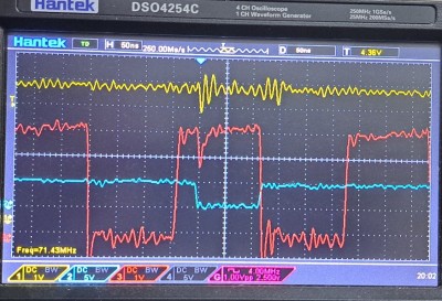
The top, yellow trace is VCC, measured at an extreme point on the circuit, a long way from the power supply. It is actually even worse in some other parts of the circuit but this happens to be what I was probing when I captured the traces. The trigger is set to 4.36V here; generally I tweaked it until the scope triggered fairly often, but not all the time, so that I could be reasonbly confident I was looking at the same artifact each time.

The red trace that goes up and down a lot is the /COE signal which drives the counters' output-enable pins and the video RAM's output-enable pin. It's at 1V per division, so it's swinging over about 4V. It cycles every four VGA pixels - for four of them these chips are outputting, and for the remaining four they are not; and during those remaining four, sometimes, a write occurs instead. Otherwise the buses float. It is tempting to add a pull-up to this line, to help it get up nearer 5V, as the counters are HC devices not HCT. Although the GALs don't always pull all the way up to 5V, they are quite good at pulling down to 0V, so the pull-up resistor does a good job of fixing the high levels without harming the low levels.

The blue trace that is set to 5V per division shows the opposite output-enable signal - /XOE. This was originally named as the output-enable for some transceivers, but they've been replaced with registers now. These drive the video address and data buses during write operations, whereas during the read half of the cycle the counters drive the video address bus and the RAM drives the video data bus. The start of this signal is delayed slightly after the end of /COE (red trace) and you can see that when it does start, that's where the dip and instability in VCC occurs. There is also some instability in VCC at the opposite end, where /XOE ends and /COE starts again. Unlike the red trace, the blue one is managing a good 5V swing - it is driving far fewer ICs though.

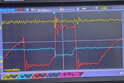
There is not much more I can do in terms of decoupling for these chips - some artifacts like these are inevitable on breadboards. It is possible that using HC registers rather than the current 74AHC574 ones would be a better choice though, as it appears the drop in VCC is due to these registers driving the video buses. Indeed, probing lines on the video data bus shows that they are all rising from low to high at the point of the instabliity - so it seems more related to the video data bus than the video address bus.

I don't have 74HC574s, but I do have some 74HCT374s, so I swapped the data bus register (U9) over to one of those - but it did not seem to reduce the voltage drop. The only thing I've found which does help here is to add pull-up resistors to some of the video data bus lines (pins 12-19 on U9) - adding one low-value resistor like 470 ohms stopped the visible artifacts on screen, and adding three or four higher value resistors (5K6) was also enough to remove the visible artifacts. I think the reason this helps is that after /COE ends, this bus is floating, and the resistors can start to pull it up a bit, meaning that when /XOE begins the data bus line is already nearer its target voltage level.
Attachment:
20231230_121729.jpg
20231230_121729.jpg [ 260.35 KiB | Viewed 446 times ]

This solution isn't great, but may be the most that can be done on a breadboard without expanding the circuit a lot. I expect these issues will get better when this is on a PCB, as it'll be possible to provide better decoupling and ground return paths between the relevant ICs, and reduce the amount of wiring in the bus itself to reduce its overall capacitance.

Another option that sprang to mind was to insert small series resistors between the tristate register's output pins and the data bus lines, to reduce the transient currents when the register's outputs are enabled. I believe this would have helped, but there's no space for that on the crowded breadboard.

Finally I could change the way the bus multiplexing works, to use multiplexers instead of tristate devices, as Jeff has suggested in other threads. Whether that helps with this issue will depend on the multiplexer, but a big advantage there is that the bus that's being driven would be very short, so easier to drive back and forth.

Any other thoughts on solutions are welcome, but in general I'm happy to leave this as it is, with the pull-up resistors, and when I expand it to support text attributes, or make a graphics-based version, then I can consider either making space for the series resistors, or using multiplexers or another solution instead.


Top
 Profile  
Reply with quote  
PostPosted: Sat Dec 30, 2023 5:36 pm 
Offline
User avatar

Joined: Thu Dec 11, 2008 1:28 pm
Posts: 10793
Location: England
Does this boil down to the databus drivers having high edge rates and therefore causing quite a disturbance? If there's no easy way to choose weaker drivers, then the small series resistor solution sounds good to me - other than there being no room for them!

Another nice analysis though. (You don't say what the vertical scale is for the yellow VCC trace, I think.)


Top
 Profile  
Reply with quote  
PostPosted: Sat Dec 30, 2023 5:49 pm 
Offline

Joined: Fri Dec 21, 2018 1:05 am
Posts: 1076
Location: Albuquerque NM USA
Does the problem get better or worse when you change supply voltage? It is a global way of assessing whether you have a performance issue or system noise problem.
Bill


Top
 Profile  
Reply with quote  
PostPosted: Sat Dec 30, 2023 5:51 pm 
Offline
User avatar

Joined: Thu May 28, 2009 9:46 pm
Posts: 8147
Location: Midwestern USA
plasmo wrote:
Does the problem get better or worse when you change supply voltage? It is a global way of assessing whether you have a performance issue or system noise problem.
Bill

Also, what is being used as the power source?

_________________
x86?  We ain't got no x86.  We don't NEED no stinking x86!


Top
 Profile  
Reply with quote  
PostPosted: Sat Dec 30, 2023 8:46 pm 
Offline

Joined: Fri Jul 09, 2021 10:12 pm
Posts: 741
The supply I'm using is a generic DC barrel jack supply with several output options, set to 5V but it generally outputs about 5.3V. I can't easily hook up to a bench supply at the moment to test whether that helps, or to test varying voltages. The vertical scale for the VCC trace was 1V per division, so from the photos it looks like it is generally hovering between 5V and 5.4V, except during the glitches. It wasn't shown in the traces I posted, but the VCC noise is especially present at the power pins of the registers, even more prominently than what I was probing before; and the voltage near the supply doesn't have these glitches on it.

Regarding the driver strength, for this kind of application I do usually want the fast transitions, hence using the AHC registers by default - however, this circuit is running at about half of the speed I usually do, as the read/write cycle is eight VGA pixels long rather than just four, so slower drivers should be able to work fine in this circuit. After the register's output-enable, it has 40ns to put a clean address onto the bus before the RAM's write-enable goes low, and then another 40ns before both signals end again; and the RAM itself only needs less than 10ns of write pulse with valid address and data, so there's a lot of spare time to leave room for slower edges. However, switching to HCT didn't seem to help in this case.

I am surprised at the level of drain from the video data bus register, given that its eight output pins are each only going to two other devices - to the data pins of a RAM IC with its outputs disabled, and to the address pins of an EEPROM, both of which are connected with quite short wires. It is not really a lot of load to have to charge up! So I may build a separate circuit to test just this bus driving issue, without the complexities of the rest of the system, as it's hard to diagnose it further in situ. It will be good at least to verify in isolation whether using multiplexers instead works better, then I can design that into the next one.


Top
 Profile  
Reply with quote  
PostPosted: Sun Dec 31, 2023 12:30 am 
Offline

Joined: Sun Sep 24, 2023 3:45 pm
Posts: 45
Awsome project!
Have you considered using a FIFO like CD74HC40105 instead of registers? Edit.. You'd need to keep the parellel to serial register and put the Fifo in front using the Fifo Not Empty to decide to gate in another update.
You would still need to be mindful of sending updates too fast but you would also still eliminate a lot of timing issues.
The 'empty' and 'full' signals could be of use I'd think. You could expose them with a register to the cpu and poll to update?


Top
 Profile  
Reply with quote  
PostPosted: Sun Dec 31, 2023 3:40 am 
Offline
User avatar

Joined: Fri Aug 03, 2018 8:52 am
Posts: 745
Location: Germany
alternatively, the IDT720x series would also be an option. being 9 bits wide instead of 4 and having a greater depth.

overall FIFOs are quire useful for Video circuits as they allow you to sort-of parallelize operations that would usually be done in series. like fetching bytes from RAM and pushing out bytes to the screen.

for example (if i read your posts and schematic right), your circuit does the following every 8 cycles:
  • read a byte from RAM, this is the ID of the character to be drawn
  • use the ID plus the current lower nibble of the Y coordinate to load a slice of the character from ROM into the shift register
  • shift out the character slice

so one idea would be to place a FIFO between the databuses of U1 (VRAM) and U2 (Character ROM), which by itself wouldn't do much. but it does seperate the Sync counters from the video address generation, meaning you could use a seperate counter to access VRAM and load bytes into the FIFO.
obviously that would add components and complexcity, but it would also allow for 2 things that work pretty well together.
for one, you could run the fetching of bytes from VRAM much much faster than the rest of the video circuit, keeping the FIFO nice and full.
and two, when the CPU wants to access VRAM you only need to deal with the Video address counter and it's FIFO instead of the entire video circuit. meaning you could just pause the Video address counter and give the CPU full access to VRAM for it's cycle as the FIFO is likely full enough to supply the video circuit with valid data until the CPU is done.

In theory that should completely avoid the issue of writes getting ignored while also giving the CPU the ability to read from VRAM as well.

another idea, which NormalLuser suggested, is to replace the register U9 with a FIFO. though i'd go further and say to use 3 FIFOs. 1 to hold the data to be written, and the other 2 hold the address where to write the data to.
so when the CPU wants to write to VRAM both the data and the address will be captured, and during unused cycles the video circuit can just seperate itself from the address and data lines of the VRAM, and read from all 3 FIFOs at once to relay the CPU's writes directly to the VRAM.
that also means you technically don't need U7 and U8 anymore (if you were to make use of the H/V-counter's CE pin to tri-state them while the FIFOs output the address, otherwise you still need them between the counters and the VRAM address lines).

anyways those are just my thoughts!


Top
 Profile  
Reply with quote  
PostPosted: Sun Dec 31, 2023 2:58 pm 
Offline

Joined: Fri Jul 09, 2021 10:12 pm
Posts: 741
Yes I am interested in the options for using FIFOs here - we discussed these things a bit a few months ago on this thread and I posted a 40105-based design there. To some extent my current circuit is a stepping stone to that - my existing VGA prototype wasn't working well any more, and I wanted to make a new version with an asynchronous interface, and try out a few options there. I haven't thought much about putting the FIFO after the RAM, though.


Top
 Profile  
Reply with quote  
PostPosted: Mon Jan 01, 2024 7:23 pm 
Offline

Joined: Sat Oct 28, 2023 7:57 pm
Posts: 15
Location: Missouri
Just wanted to say thanks for posting this (and for the answer on the CPLD question I asked a bit earlier). I'm looking at designing a rather convoluted video setup with some complex timing, and your experience here is proving very valuable reading!


Top
 Profile  
Reply with quote  
Display posts from previous:  Sort by  
Post new topic Reply to topic  [ 25 posts ]  Go to page Previous  1, 2

All times are UTC


Who is online

Users browsing this forum: No registered users and 37 guests


You cannot post new topics in this forum
You cannot reply to topics in this forum
You cannot edit your posts in this forum
You cannot delete your posts in this forum
You cannot post attachments in this forum

Search for:
Jump to: