6502.org Forum  Projects  Code  Documents  Tools  Forum
It is currently Sat Apr 27, 2024 6:14 pm

All times are UTC


Post new topic Reply to topic  [ 21 posts ]  Go to page 1, 2  Next
Author Message
PostPosted: Mon Nov 27, 2023 8:46 pm 
Offline
User avatar

Joined: Fri Feb 17, 2023 11:59 pm
Posts: 163
Location: Lviv, Ukraine
I actually love bit-banging, but it's really slow for the kind of project I'm doing which involves reading large quantities of data from SD card.

Now, this is definitely not the most optimal solution, but it's been working correctly in simulations and I'm honestly proud of it! So here I am, bragging about it. :lol:

FYI, chip selection logic is not handled here and is left to be handled by other means.

In total, 3 chips are used: '04, '191, & '299. (Well, /BUSY still needs to be memory-mapped somewhere...)

Attachment:
spi.png
spi.png [ 132.92 KiB | Viewed 3602 times ]


Why not use e. g. 65SPI? Because of DIP. I have a fetish for DIP, and I want all my stuff in DIP!
Additionally, I'm planning to use this not only with 65xx-based systems, but with x86 SBC as well.

Finally, I find spending late nights designing circuits in Digital a relaxing experience, even if they don't do much useful stuff.

EDIT: Now that I think of it, it might be possible to implement all of this in 2 GALs.


Attachments:
File comment: Circuit for Digital (https://github.com/hneemann/Digital)
spi.zip [113.58 KiB]
Downloaded 39 times

_________________
/Andrew

deck65 - 6502 slab with screen and keyboard | ПК-88 - SBC based on KM1810VM88 (Ukrainian i8088 clone) | leo80 - simple Z80 SBC
nice65 - 6502 assembly linter | My parts, footprints & 3D models for KiCad/FreeCAD
Top
 Profile  
Reply with quote  
PostPosted: Mon Nov 27, 2023 9:03 pm 
Offline

Joined: Tue Jul 05, 2005 7:08 pm
Posts: 990
Location: near Heidelberg, Germany
This is actually quite nice!

I wonder, should busy (when not busy) not also be used to disable SCK, so every write will trigger exactly 8 pulses on SCK? Otherwise you have to time each write exactly or count clk separately? When disabling SCK when not busy you could even use a continuous clock like phi2 as clk.

Also, what SPI mode does it implement? The relationship between SCK and output bits is sometimes difficult depending on used shift register chip

_________________
Author of the GeckOS multitasking operating system, the usb65 stack, designer of the Micro-PET and many more 6502 content: http://6502.org/users/andre/


Top
 Profile  
Reply with quote  
PostPosted: Tue Nov 28, 2023 12:54 am 
Offline
User avatar

Joined: Fri Feb 17, 2023 11:59 pm
Posts: 163
Location: Lviv, Ukraine
fachat wrote:
This is actually quite nice!

I wonder, should busy (when not busy) not also be used to disable SCK, so every write will trigger exactly 8 pulses on SCK? Otherwise you have to time each write exactly or count clk separately? When disabling SCK when not busy you could even use a continuous clock like phi2 as clk.

Also, what SPI mode does it implement? The relationship between SCK and output bits is sometimes difficult depending on used shift register chip


Thanks! Yeah, in my design clock is supposed to come from Ф2. I was implementing SPI mode 0, however I did several mistakes. Here's the (hopefully) fixed diagram. I had to introduce a pair of OR gates to qualify reads/writes with chip selection. There could be a better way that I'm not seeing!
Attachment:
spi3b.png
spi3b.png [ 172.78 KiB | Viewed 3540 times ]


I've also added built-in test cases that you can run with Digital. Timing diagram from built-in test case looks as such (sending 00011101, receiving 11100010):
Attachment:
spi3a.png
spi3a.png [ 30.62 KiB | Viewed 3540 times ]


Updated schematic:


Attachments:
File comment: Circuit for Digital (https://github.com/hneemann/Digital)
spi.zip [2.7 KiB]
Downloaded 36 times

_________________
/Andrew

deck65 - 6502 slab with screen and keyboard | ПК-88 - SBC based on KM1810VM88 (Ukrainian i8088 clone) | leo80 - simple Z80 SBC
nice65 - 6502 assembly linter | My parts, footprints & 3D models for KiCad/FreeCAD


Last edited by and3rson on Tue Nov 28, 2023 11:16 am, edited 2 times in total.
Top
 Profile  
Reply with quote  
PostPosted: Tue Nov 28, 2023 6:23 am 
Offline

Joined: Wed Aug 21, 2019 6:10 pm
Posts: 217
and3rson wrote:
... There could be a better way that I'm not seeing! ...


Not better as such, but it seems like, if there are two selects that can be used, and the select does not lead the drop of R/W, an alternate way to generate the clock is from the write select, so that the select itself is the chip serial clock and the select OR'd with the inverse of R/W for the SPI clock, so that eight reads from the "write" I/O address provides the clock pulses.

But that is a mode3 cycle, and if a mode 0 is what is wanted, then when you add a GPIO somewhere plus a 74x00 convert the mode 3 SPI_SCLK to a mode 0 SPI_SCLK, you've added back in any glue logic you've saved by using the select as an SCLK.


Top
 Profile  
Reply with quote  
PostPosted: Tue Nov 28, 2023 7:10 am 
Offline

Joined: Tue Jul 05, 2005 7:08 pm
Posts: 990
Location: near Heidelberg, Germany
Just a quick reply

I have to look at the specs... is SPI lsb first?

I think you can get to mode 0 if you OR ph2 and /busy to get SCK.

_________________
Author of the GeckOS multitasking operating system, the usb65 stack, designer of the Micro-PET and many more 6502 content: http://6502.org/users/andre/


Top
 Profile  
Reply with quote  
PostPosted: Tue Nov 28, 2023 8:39 am 
Offline
User avatar

Joined: Fri Aug 30, 2002 1:09 am
Posts: 8428
Location: Southern California
fachat wrote:
I have to look at the specs... is SPI lsb first?

No.  msb first..

_________________
http://WilsonMinesCo.com/ lots of 6502 resources
The "second front page" is http://wilsonminesco.com/links.html .
What's an additional VIA among friends, anyhow?


Top
 Profile  
Reply with quote  
PostPosted: Tue Nov 28, 2023 11:19 am 
Offline
User avatar

Joined: Fri Feb 17, 2023 11:59 pm
Posts: 163
Location: Lviv, Ukraine
Oops, that's embarassing - I've updated my post with corrected images & circuit file. I could've sworn there was a ROR in my code, but it is indeed ROL... :D

fachat wrote:
I think you can get to mode 0 if you OR ph2 and /busy to get SCK.


Yeah - that's how I did it in my schematic.

_________________
/Andrew

deck65 - 6502 slab with screen and keyboard | ПК-88 - SBC based on KM1810VM88 (Ukrainian i8088 clone) | leo80 - simple Z80 SBC
nice65 - 6502 assembly linter | My parts, footprints & 3D models for KiCad/FreeCAD


Top
 Profile  
Reply with quote  
PostPosted: Tue Nov 28, 2023 12:24 pm 
Offline

Joined: Tue Jul 05, 2005 7:08 pm
Posts: 990
Location: near Heidelberg, Germany
and3rson wrote:
Oops, that's embarassing - I've updated my post with corrected images & circuit file. I could've sworn there was a ROR in my code, but it is indeed ROL... :D


I didn't look at your code, but if I get it right this should depend on the shift direction of your shift register? But you could also invert the wiring... like D0->SR7, D1->SR6,....
Quote:

fachat wrote:
I think you can get to mode 0 if you OR ph2 and /busy to get SCK.


Yeah - that's how I did it in my schematic.


The schematics shows and AND with busy, if I'm not mistaken. So inactive SCK becomes low. Which is mode CPOL=0 ok for mode 0. I was mistaken because I usually do mode 3....
Btw your MOSI in the simulation above seem to be running in CPHA=0, making it mode 0. Your MISO seems to be running in CPHA=1?

Edit:
Note that compatibility can strongly depend on which mode the attached device supports. Most that I use support mode 0 and 3, as they sample on the rising edge and put out a new bit on the falling edge, but there are others.

Edit 2: https://en.m.wikipedia.org/wiki/Serial_ ... _Interface

_________________
Author of the GeckOS multitasking operating system, the usb65 stack, designer of the Micro-PET and many more 6502 content: http://6502.org/users/andre/


Top
 Profile  
Reply with quote  
PostPosted: Tue Nov 28, 2023 7:33 pm 
Offline
User avatar

Joined: Fri Feb 17, 2023 11:59 pm
Posts: 163
Location: Lviv, Ukraine
fachat wrote:
I didn't look at your code, but if I get it right this should depend on the shift direction of your shift register? But you could also invert the wiring... like D0->SR7


Yes, that's correct - I was just joking that while converting my existing bit-banging code into this schematic, I misread ROL as ROR and thus assumed that SPI sends LSB first - hence my error. I fixed this by changing the direction of '299.

fachat wrote:
The schematics shows and AND with busy, if I'm not mistaken. So inactive SCK becomes low. Which is mode CPOL=0 ok for mode 0. I was mistaken because I usually do mode 3....
Btw your MOSI in the simulation above seem to be running in CPHA=0, making it mode 0. Your MISO seems to be running in CPHA=1?

Edit:
Note that compatibility can strongly depend on which mode the attached device supports. Most that I use support mode 0 and 3, as they sample on the rising edge and put out a new bit on the falling edge, but there are others.

Edit 2: https://en.m.wikipedia.org/wiki/Serial_ ... _Interface


Ah, yes, that's right. Sorry, I misread your message.
There indeed is an issue here with MISO being sampled on the falling edge, and it affects both modes 0 (AND) & 3 (OR). Main challenge here is that in mode 3, MOSI needs to be shifted out on FALLING edge of the clock, but MISO needs to be shifted in on RISING edge.
I think I could get away by simply adding 2 of remaining inverters as a buffer between MISO & '299 DSR input (to ensure that MISO is still valid even on falling edge of SCK). A better way would be to use a D flip-flop, but this adds one more chip to the mix.

_________________
/Andrew

deck65 - 6502 slab with screen and keyboard | ПК-88 - SBC based on KM1810VM88 (Ukrainian i8088 clone) | leo80 - simple Z80 SBC
nice65 - 6502 assembly linter | My parts, footprints & 3D models for KiCad/FreeCAD


Top
 Profile  
Reply with quote  
PostPosted: Wed Nov 29, 2023 12:51 am 
Offline
User avatar

Joined: Fri Feb 17, 2023 11:59 pm
Posts: 163
Location: Lviv, Ukraine
Somewhat off-topic: I recently discovered ATF750 & ATF2500 (https://eu.mouser.com/ProductDetail/Mic ... GZiw%3D%3D). They are in DIP, Microchip still makes them, and they are basically 22V10 with additional 10 buried registers - that's plenty enough to implement a lot of things in a single chip. Buried registers can be used for counter & BUSY in this case, and output registers - for shift register.

I'm also going back to WinCUPL since galasm, galette, and palwiz all suffer from the same problem - incorrect and ambiguous handling of inverted registers (https://github.com/daveho/GALasm/issues/16). I tried to fix it in galasm, but didn't get any stable results. I'm still going to use galasm occasionally for simple equations.
TL;DR: WinCUPL generates the fuses exactly how I expect them, while galasm/galette/palwiz don't. Though I still wish WinCUPL's UI did not suck so hard under Wine though... But hey - at least it works!

</rant>

EDIT: Seems like I'll have hard time programming ATF750... viewtopic.php?f=10&t=4323&p=104766#p104766

_________________
/Andrew

deck65 - 6502 slab with screen and keyboard | ПК-88 - SBC based on KM1810VM88 (Ukrainian i8088 clone) | leo80 - simple Z80 SBC
nice65 - 6502 assembly linter | My parts, footprints & 3D models for KiCad/FreeCAD


Top
 Profile  
Reply with quote  
PostPosted: Wed Nov 29, 2023 2:28 am 
Offline

Joined: Fri Jul 09, 2021 10:12 pm
Posts: 741
Quote:
Though I still wish WinCUPL's UI did not suck so hard under Wine though... But hey - at least it works!
WinCupl's GUI socks even in native Windows - it is awful and crashes a lot. I'm not sure if I said to you before, but I use WinCupl from the command line instead. At first using cygwin, but later using Wine. I use a bash script to wrap the tool and make it behave a bit better, putting generated files away from the source code, spreading useless output, etc. It has made my life a lot easier.

Quote:
EDIT: Seems like I'll have hard time programming ATF750... viewtopic.php?f=10&t=4323&p=104766#p104766
The newer version of the TL866 - the T56 - can program them. It's not cheap but I've heard good things about the device. However, I don't believe there is any Linux software for it, you'd need to use the Windows software.


Top
 Profile  
Reply with quote  
PostPosted: Wed Nov 29, 2023 3:37 am 
Offline

Joined: Wed Aug 21, 2019 6:10 pm
Posts: 217
and3rson wrote:
... Main challenge here is that in mode 3, MOSI needs to be shifted out on FALLING edge of the clock, but MISO needs to be shifted in on RISING edge. ...


That's the kind of issue that leads some people to using separate MISO and MOSI serial shift registers, which can be clocked on PHI1 or PHI2 as works best for that side of the operation.

If using a latch, since there are dual '74 clocked latches with direct and inverse outputs and /clear and /preset, perhaps there is a way to use the other side of the latch to eliminate some of the other logic.

This uses the /USR_Write_Select = OR(R/W,/EN) directly as much as possible.

/COUNT_LOAD := OR(R/W,/EN) ; Load counter when MOSI byte is loaded.
COUNT_CP := PHI2 ; do count in between USR shifts
COUNT_CLR := /LATCH_1Q ; hold counter clear outside of SPI byte counting state

; Push LATCH_1Q high, /LATCH_1Q low when USR is written. 1Q is the state for running the counter.
/LATCH_1PRE := OR(R/W,/EN)
/LATCH_1CLR := /COUNT_CO ; Finish the state for running the counter

; Latch 2 holds MOSI bit
LATCH_2D := USR_Q7
LATCH_2CP := PHI2
LATCH_2Q =: SPI_MOSI

PHI1_SCLK := NAND(PHI2,LATCH_1Q)

/USR_S1 := OR(R/W,/EN) ; Load data into USR_Q1-USR_Q7
USR_CP := PHI1_SCLK ; run USR in sync with SPI bus

The first PHI1_SCLK clock tick is for loading, not for the SPI bus. This cleans that out. Also, this introduces two gate delays between PHI1_SCLK and PHI1_SPI_SCLK, which means MISO has been shifted in by the USR before the SPI shifts the next MISO bit onto the line:
PHI1_SPI_SCLK := NOT(NAND(PHI1_SCLK,NOT(R/W)))

I think the Counter is loaded with $7, but I'm not sure: for a '193, load is asynchronous, so the rising Phi2 before the USR is loaded won't tick the counter, so I think it's 1 tick before each shift and then one tick following the last shift. Since a carry overflow is being used rather than the state of the counter Q3, it's not required to count to exactly eight.

Since it's system clocked, it doesn't seem crucial to have a Busy status, just add three NOPs between writing the output byte and reading the input byte, the eighth SPI clock cycle will be finished before the final clock cycle of the read.

For getting the part count down, since there are two NAND gates already used and two NOT, the two OR gates might be replaced by A+B = /(/A*/B)

EN := NOT(/EN)
W/R := NOT(R/W)
/EN_WR := NAND(EN,W/R)
/EN_RD := NAND(EN,R/W)

... and two gates from a hex inverter are still available if it is needed to add another delay.


Top
 Profile  
Reply with quote  
PostPosted: Wed Nov 29, 2023 11:50 pm 
Offline
User avatar

Joined: Fri Feb 17, 2023 11:59 pm
Posts: 163
Location: Lviv, Ukraine
gfoot wrote:
Quote:
Though I still wish WinCUPL's UI did not suck so hard under Wine though... But hey - at least it works!
WinCupl's GUI socks even in native Windows - it is awful and crashes a lot. I'm not sure if I said to you before, but I use WinCupl from the command line instead. At first using cygwin, but later using Wine. I use a bash script to wrap the tool and make it behave a bit better, putting generated files away from the source code, spreading useless output, etc. It has made my life a lot easier.

Quote:
EDIT: Seems like I'll have hard time programming ATF750... viewtopic.php?f=10&t=4323&p=104766#p104766
The newer version of the TL866 - the T56 - can program them. It's not cheap but I've heard good things about the device. However, I don't believe there is any Linux software for it, you'd need to use the Windows software.


Thanks - I've ordered T56 today because I'm a sucker for DIP PLD chips. I managed to get WinCUPL (somewhat) working and even got used to its terrible pet peeves, learning what not to do in order to keep it from crashing. :lol:

BruceRMcF wrote:
That's the kind of issue that leads some people to using separate MISO and MOSI serial shift registers, which can be clocked on PHI1 or PHI2 as works best for that side of the operation.

If using a latch, since there are dual '74 clocked latches with direct and inverse outputs and /clear and /preset, perhaps there is a way to use the other side of the latch to eliminate some of the other logic.


Yeah, a latch to buffer MISO is definitely the missing link.
BruceRMcF wrote:
The first PHI1_SCLK clock tick is for loading, not for the SPI bus


Yeah, I just realized this today when I was trying to implement my circuit with ATF750C - I had to use modulo-9 counter to properly time everything, including the last clock tick which is easy to miss.
BruceRMcF wrote:
I think the Counter is loaded with $7, but I'm not sure: for a '193, load is asynchronous, so the rising Phi2 before the USR is loaded won't tick the counter, so I think it's 1 tick before each shift and then one tick following the last shift. Since a carry overflow is being used rather than the state of the counter Q3, it's not required to count to exactly eight.


For my circuit, I swapped '163 & '191 in and out, trying to find the best fit, but I was always lacking an additional asynchronous reset/preset. Still, your idea sounds nice!

BruceRMcF wrote:
Since it's system clocked, it doesn't seem crucial to have a Busy status, just add three NOPs between writing the output byte and reading the input byte, the eighth SPI clock cycle will be finished before the final clock cycle of the read.


Totally! I decided to ditch that output as well, since NOPs are sufficient for proper delay (which is constant) and simplifies the design.

I eventually implemented my design into ATF750C, and this is probably my most complex PLD project so far:

Code:
Name     SPI;
PartNo   00;
Date     29.11.2023;
Revision 01;
Designer Engineer;
Company  Andrew;
Assembly None;
Location ;
Device   v750;

/* Unused pins for nicer group separation in simulator */
pin 7  = NOP1;
pin 8  = NOP2;
pin 9  = NOP3;

/* Inputs */
pin 1   = CLK;
pin 2   = !RD;
pin 3   = !WR;
pin 4   = !CS;
pin 5   = !RES;
pin 6   = MISO;
pin 13  = !EN;

/* Bidirectional */
pin 14  = D0;
pin 15  = D1;
pin 16  = D2;
pin 17  = D3;
pin 18  = D4;
pin 19  = D5;
pin 20  = D6;
pin 21  = D7;

/* Outputs */
pin 22  = MOSI;
pin 23  = SCK;

/* Buffer for MISO */
node MISO_BUF;

/* 4-bit modulo-9 counter, active when TEN is high */
node T0;
node T1;
node T2;
node T3;
node TEN;

T0.CK  = CLK;
T0.D   = TEN & !T0 & !T3;
T1.CK  = CLK;
T1.D   = TEN & (!T1 & T0 # T1 & !T0);
T2.CK  = CLK;
T2.D   = TEN & (T2 & !T1 # T2 & !T0 # !T2 & T1 & T0);
T3.CK  = CLK;
T3.D   = TEN & (T3 # T2 & T1 & T0);
/* Timer is activated when /CS & /WR are active, and deactivated when 8 is reached. */
TEN.CK = !CLK;
TEN.D = EN & WR # (TEN & !T3);
[T0..T3].SP = 'b'0;
[T0..T3].AR = RES;
TEN.SP = 'b'0;
TEN.AR = RES;

/* Data is sampled/shifted on falling edge of CLK and is tri-stated when /EN is high or /RD is high. */
[D0..D7].OE = EN & RD;
[D0..D7].CK = !CLK;
[D0..D7].SP = 'b'0;
/* If timer is active, data is shifted. Otherwise, data is sampled if /EN & /WR active or held otherwise. */
D7.D = TEN & D6         #   !TEN & EN & WR & D7.IO   #   !TEN & (!EN # !WR) & D7; /* D7 drives MOSI */
D6.D = TEN & D5         #   !TEN & EN & WR & D6.IO   #   !TEN & (!EN # !WR) & D6;
D5.D = TEN & D4         #   !TEN & EN & WR & D5.IO   #   !TEN & (!EN # !WR) & D5;
D4.D = TEN & D3         #   !TEN & EN & WR & D4.IO   #   !TEN & (!EN # !WR) & D4;
D3.D = TEN & D2         #   !TEN & EN & WR & D3.IO   #   !TEN & (!EN # !WR) & D3;
D2.D = TEN & D1         #   !TEN & EN & WR & D2.IO   #   !TEN & (!EN # !WR) & D2;
D1.D = TEN & D0         #   !TEN & EN & WR & D1.IO   #   !TEN & (!EN # !WR) & D1;
D0.D = TEN & MISO_BUF   #   !TEN & EN & WR & D0.IO   #   !TEN & (!EN # !WR) & D0; /* D0 is shifted in from MOSI */

/* MOSI is set from D7 and is always active */
MOSI = D7;
MOSI.OE = 'b'1;

/* MISO is sampled on rising edge of CLK. */
MISO_BUF.CK = CLK;
MISO_BUF.SP = 'b'0;
MISO_BUF.D  = MISO;

/* SCK is set from CLK, but only when timer is active */
SCK = CLK & TEN;


Test vertors:

Code:
Name     SPI;
PartNo   00;
Date     29.11.2023;
Revision 01;
Designer Engineer;
Company  Andrew;
Assembly None;
Location ;


ORDER: CLK, !RES, !EN, !RD, !WR, NOP1, D0, D1, D2, D3, D4, D5, D6, D7, NOP2, MISO, MOSI, SCK, NOP3, T0, T1, T2, T3, TEN;


VECTORS:
0K111XZZZZZZZZX1**X*****
C1111XZZZZZZZZX1**X*****
11010XZZZZZZZZX1**X*****
01010X01100011X1**X*****
01001X********X0**X*****
11001X********X0**X*****
01001X********X1**X*****
11001X********X1**X*****
01001X********X0**X*****
11001X********X0**X*****
01001X********X1**X*****
11001X********X1**X*****
01001X********X0**X*****
11001X********X0**X*****
01001X********X0**X*****
11001X********X0**X*****
01001X********X1**X*****
11001X********X1**X*****
01001X********X1**X*****
11001X********X1**X*****
01001X********X0**X*****
11001X********X0**X*****
01001X********X0**X*****
11001X********X0**X*****
01001X********X0**X*****
11001X********X0**X*****
01001X********X0**X*****
11001X********X0**X*****
01001X********X0**X*****


Result (sending 11000110, receiving 01010011):


It currently works in SPI mode 0 only, but I was thinking of trying to implement all 4 modes which can be configured by writing to a different address. There's still plenty of buried registers for this, but I'm afraid I might run into the term limit, since changing CPOL & CPHA will require some heavy XOR-ing which cupl might not like... :)
Attachment:
spi4.png
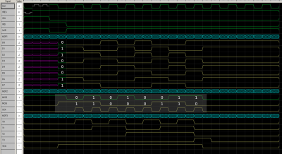
spi4.png [ 461.57 KiB | Viewed 3426 times ]

_________________
/Andrew

deck65 - 6502 slab with screen and keyboard | ПК-88 - SBC based on KM1810VM88 (Ukrainian i8088 clone) | leo80 - simple Z80 SBC
nice65 - 6502 assembly linter | My parts, footprints & 3D models for KiCad/FreeCAD


Top
 Profile  
Reply with quote  
PostPosted: Thu Nov 30, 2023 12:52 am 
Offline

Joined: Fri Jul 09, 2021 10:12 pm
Posts: 741
Nice. My current SD solution is an ATF22V10 driving two shift registers (one in, one out) with an additional 74HC139 - it provides a read/write I/O address and a status I/O address, and writing the status address sets CS high or low. I can share the design more if you like, perhaps you can get the ATF750 to do all of it in one chip. It is quite pleasant to use from code.


Top
 Profile  
Reply with quote  
PostPosted: Thu Nov 30, 2023 4:15 am 
Offline

Joined: Wed Aug 21, 2019 6:10 pm
Posts: 217
and3rson wrote:
BruceRMcF wrote:
... I think the Counter is loaded with $7, but I'm not sure: for a '193, load is asynchronous, so the rising Phi2 before the USR is loaded won't tick the counter, so I think it's 1 tick before each shift and then one tick following the last shift. Since a carry overflow is being used rather than the state of the counter Q3, it's not required to count to exactly eight.


For my circuit, I swapped '163 & '191 in and out, trying to find the best fit, but I was always lacking an additional asynchronous reset/preset. Still, your idea sounds nice! ...


If the state machine works correctly, the SPI clock only ever cycles after a write of a byte into the USR, and always stops after a full byte has been written out on MOSI and read into the USR from MISO, which can be read multiple times, but will be replaced by the next write before the SPI clock cycles again ... so there is no need to reset/preset the shift register.


Top
 Profile  
Reply with quote  
Display posts from previous:  Sort by  
Post new topic Reply to topic  [ 21 posts ]  Go to page 1, 2  Next

All times are UTC


Who is online

Users browsing this forum: Proxy and 39 guests


You cannot post new topics in this forum
You cannot reply to topics in this forum
You cannot edit your posts in this forum
You cannot delete your posts in this forum
You cannot post attachments in this forum

Search for:
Jump to: