6502.org Forum  Projects  Code  Documents  Tools  Forum
It is currently Fri May 10, 2024 1:20 am

All times are UTC


Post new topic Reply to topic  [ 7 posts ] 
Author Message
PostPosted: Fri Sep 29, 2023 10:44 pm 
Offline

Joined: Fri Jul 09, 2021 10:12 pm
Posts: 741
I've posted some of this circuit before but I've now refreshed and fixed it up. It's not working 100% but is getting there and I thought it'd be good to give it its own thread, recap some of the background, show the circuit, and explain how it works and where some problems still seem to lie.

The Cypress FX2 EZ-USB logic analyser combined with hoglet's 6502 decoder (https://github.com/hoglet67/6502Decoder ... -Analyzers) is great for capturing what a 6502 system is doing and debugging it. However at clock frequencies above maybe 12-16MHz, especially combined with clock stretching or use of RDY (including WAI and STP), it can be hard to get it to work, and I've been iterating on this adaptor circuit to help out with that.

It works fairly well at the moment but I still have some problems at 32MHz clock speed, which look like they're due to data loss between the logic analyser and the PC. About 75% of my captures seem to be fine, but maybe 25% of them have some form of error during the course of 200 million samples, that often turns out to be a correct-looking data stream but with a sequence of bytes missing. It's possible that some OS priority tweaks might resolve it, but equally this may just be the limit of what's possible over USB2 - I haven't fully diagnosed that yet.

Nonetheless, here's the circuit that I'm now using, with some explanation:

Attachment:
File comment: Logic analyser hat schematic (work in progress)
logicanalyserhat-schematic-partial.png
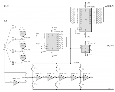
logicanalyserhat-schematic-partial.png [ 43.25 KiB | Viewed 3213 times ]


Dave has documented various ways to configure the FX2 that are appropriate for different clock rates. In particular, I'm focusing on clock speeds above about 16MHz, which require you to run the logic analyser in "Slave FIFO Synchronous Write" mode, driven by an external clock (e.g. PHI2), with 8-bit data captures (just the data bus, no control signals). This works because the logic analyser only captures one data bus sample per 6502 clock cycle, timed at the right point in the clock cycle, so there's no need to capture the clock. The decoder can reconstruct signals like RWB and SYNC, along with the whole address bus, in most cases.

There are further problems though if the 6502-based system uses clock stretching, or RDY - and note that WAI and STP rely on RDY. In the case of clock stretching, the issue is that the FX2 requires that the externally-provided clock runs at a rate of at least something like 5MHz, and it's very easy for a stretched clock to have either the high or low period of the clock be longer than what the FX2 can support. In the case of use of RDY the problem is that while the clock keeps ticking, the CPU is not progressing to the next cycle, and so the logic analyser captures unwanted duplicate data bus values during the wait period.

The solution to both problems is to provide the logic analyser with a consistent, unstretched, fast enough clock, but supply an extra signal to inhibit data bus capture on clock cycles where the CPU is paused - either because the CPU's clock is being stretched (held high) or because the CPU's RDY pin is low. I also blend in the CPU's RESET signal because it is tidier to also not capture data bus samples during the reset period - it means your decoded captures start straight from the reset with no garbage before it.

To do this we need to feed a signal into the FX2's SLWR (SLave WRite) pin (also known as RDY1). In the inverted clock mode we're using (--ifclk=xi) this appears to be active-low, though that conflicts with the documentation. SLWR has setup and hold time requirements (12.1ns and 3.6ns) compared to the IFCLK signal, so this decision needs to be made early enough to meet those. To simplify this, I am supplying a delayed or inverted clock signal to IFCLK, so that the sample is taken at a much later time (around the rising edge of PHI2) and I'm using an 8-bit D flipflop register to capture the data bus state until this point. In addition I'm using a D flipflop to capture the combination of RDY, RESET, and any clock-stretching signal, to provide the logic analyser's SLWR input, telling it whether to capture data this cycle or not. The delayed IFCLK is meant to allow this to meet the 12.1ns setup requirement of the FX2.

I used a 138 decoder to provide the input for that D flipflop, allowing a fairly arbitrary combination of the inputs to be chosen with different polarities. I want to only capture when RESET is high, RDY is high, and IO is low. IO is a signal used in my 6502 computer circuit to trigger clock stretching, and it changes while the input clock is high, making it work well for this purpose. Other 6502 computer designs will need to provide different inputs there, so the flexibility of the 138 decoder could be useful for them.

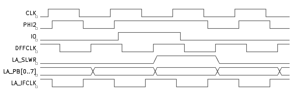
This is a timing diagram for my current setup, with IFCLK and DFFCLK driven by the closed jumpers shown in the schematic:

Attachment:
File comment: Timing diagram
logicanalyserhat-timing.png
logicanalyserhat-timing.png [ 4.5 KiB | Viewed 3213 times ]


Note that with my 6502 system PHI2 lags the input clock slightly (it's the 74AHCT32-OR of CLK with IO), and IO changes shortly after the input clock rises. The logic analyser's IFCLK is one inverter away from the input clock, so it is roughly 180 degrees out of phase with PHI2 in general. The D flipflops are being triggered three inverter delays after the input clock falls - this seems to work well in my case. This leads to LA_SLWR and LA_PB[0..7] changing around that point, and then it's important for IFCLK's falling edge (since we're using it inverted) to fall a good distance away from there. At 32MHz, half a clock cycle is 15ns which is just about enough to satisfy the 12.1ns setup time, but still a bit borderline.

So from the logic analyser's perspective, on the falling edge of LA_IFCLK, if LA_SLWR is low, then it samples LA_PB[0..7] and queues a byte to send over USB.

Now aside from the bandwidth issue, there are a few things that don't seem right to me, so I'm still investigating them. Firstly, SLWR is meant to be active-high if IFCLK is inverted, not active-low - the diagrams in the datasheet show this clearly. Actually I strongly suspect that --ifclk=xi is causing the sampling to take place on the rising edge of the IFCLK I'm supplying, not the falling edge - i.e. the sense of the inversion in the --ifclk parameter is backwards. If I swap it for --ifclk=x, i.e. not inverted, then I need to also invert SLWR (to be active-high) for it to work. Also, with --ifclk=xi, having IFCLK and DFFCLK driven by the same inverter - so they rise at the same time as each other - gives very bad results, when that ought to be more or less ideal as with =xi it's meant to sample on the falling edge. Switching to --ifclk=x in that same connfiguration gives very good results, when it should be as bad as it gets as it should then be sampling on the rising edge of IFCLK and violating all the setup/hold times.

On the bandwidth issue, I'm considering rigging up a test case that's not built around a 6502 computer just to test the capture rate and fidelity - this worked well for me before, and it's quicker to find errors in a simpler data stream, and understand where they came from. I would really like this to work at least up to 40MHz, so that's probably the next priority for me!


Top
 Profile  
Reply with quote  
PostPosted: Fri Oct 20, 2023 9:53 am 
Offline

Joined: Fri Jul 09, 2021 10:12 pm
Posts: 741
I have been using something like this circuit for a while now with a lot of success, so I went ahead and designed a PCB for a "hat" module. I swapped to using a PLD - ATF16V8C-7 - instead of AHCT inverters and flipflop. This PLD has a slightly higher specified propagation delay than the AHCT inverters did, but works very well in my case. Where I was using three inverters in a row, giving maybe a 15ns delay according to the datasheets, I'm now using one pass through the ATF16V8C-7, which is probably around a 7ns delay I think - I ought to measure it.

This is only intended for synchronous write, external clock mode. For asynchronous mode I guess PHI2 should be ORed asynchronously with the existing SLWR calculation, and IFCLK should be disconnected. I haven't thought about it much though.

Attachment:
File comment: FX2 Hat - Top View
fx2lphat_top.jpg
fx2lphat_top.jpg [ 314.38 KiB | Viewed 3072 times ]
Attachment:
File comment: FX2 Hat - Bottom View
fx2lphat_bottom.jpg
fx2lphat_bottom.jpg [ 187.69 KiB | Viewed 3072 times ]


The electrolytic capacitor may need to be mounted on the top rather than the bottom, for clearance reasons. Other than that I think it should fit well, and I tried to keep the board outline as small as possible to make it easier to line up the pins when connecting it.

The 2x7 pin block should have a single jumper across it, and where the jumper is positioned alters the sample timing relative to the input clock. The data bus and PHI2 or similar clock signal are connected in the marked places, and EN and /EN are optional pins that you can connect signals to in order to prevent sampling on some cycles - e.g. connect /RESET to one of the EN pins on J2 so that sampling doesn't occur when /RESET is not high; similarly for RDY; but if you have an active-high clock-stretching signal, you want to connect that to one of the inverted enable pins instead, on J3.

I'd include a schematic but it's not very exciting as there are only two ICs here. The PLD is asynchronously outputting an inverted PHI2, plus five or six copies delayed by different amounts by feeding back through the array; the jumper on J8 connects one of these back to the PLD's input clock, and also to the clock signal of a '574 that's latching the data bus; and also to the FX2LP's IFCLK pin, so that it samples this half a cycle out of sync (as this clock signal was inverted).

The PLD also generates a registered SLWR signal, which is the AND of various J2 and J3 pins, with the J3 pins inverted. So this is also sampled at the same time as the data bus and held steady for the next clock cycle, satisfying the FX2's setup and hold times.

It may be better to use a CPLD with more macrocells that can do the job of both these ICs, and which is 3.3V but 5V-tolerant, removing the need to supply +5V from the system under test. But these are parts I already have and have already tested, so I'm happy to make the PCB this way for now.


Top
 Profile  
Reply with quote  
PostPosted: Wed Oct 25, 2023 12:52 pm 
Offline

Joined: Fri Jul 09, 2021 10:12 pm
Posts: 741
The PCBs came through for this, so I will assemble it this evening.

Just placing components, there are some physical size issues - it will work but is not ideal in some respects.

This is how it looks stacked on top of the FX2 board:
Attachment:
20231025_130317.jpg
20231025_130317.jpg [ 894.79 KiB | Viewed 3002 times ]


I tried to ensure both jumpers and the on/off switch were accessible, as well as this button in the corner (which I guess is a reset button?):
Attachment:
20231025_130351.jpg
20231025_130351.jpg [ 1.05 MiB | Viewed 3002 times ]


There are some clearance issues however - the bulk decoupling capacitor in the corner rests on the FX2 board's crystal:
Attachment:
20231025_130459.jpg
20231025_130459.jpg [ 1.27 MiB | Viewed 3002 times ]


This will prevent the connectors being fully-engaged, unless I mount the capacitor horizontally or use a smaller value - this one is 100uF, I have smaller 22uF ones, and I don't know how much difference this capacitor is going to make anyway.

There's also not a lot of room inside for the PLD and 74AHCT574:
Attachment:
20231025_130530.jpg
20231025_130530.jpg [ 1.59 MiB | Viewed 3002 times ]


I will need to shorten the leads on the header pins, I think. But even then, if I want to have the PLD socketed, it's going to very nearly touch the FX2 IC on the dev board:
Attachment:
20231025_131535.jpg
20231025_131535.jpg [ 961.35 KiB | Viewed 3002 times ]


But not quite, so maybe this is OK. I might just solder the PLD though as I'm unlikely to want to reprogram it.


Top
 Profile  
Reply with quote  
PostPosted: Wed Oct 25, 2023 2:12 pm 
Offline
User avatar

Joined: Fri Dec 11, 2009 3:50 pm
Posts: 3354
Location: Ontario, Canada
gfoot wrote:
I'd include a schematic but it's not very exciting

Not to worry, George. We can easily forgive this minor deficit... because the photos you posted are more than amply entertaining and intriguing! Nice work! :)

-- Jeff

_________________
In 1988 my 65C02 got six new registers and 44 new full-speed instructions!
https://laughtonelectronics.com/Arcana/ ... mmary.html


Top
 Profile  
Reply with quote  
PostPosted: Mon Dec 11, 2023 3:45 pm 
Offline

Joined: Thu Dec 26, 2002 12:29 pm
Posts: 51
Location: Occitanie, France
Quote:
I'd include a schematic but it's not very exciting as there are only two ICs here.

@gfoot : Having just stumbled upon this thread, and still rather a newbie with SPLD development (I'm getting there - slowly), I'd be interested in reading your definitions for the PLDs.
I don't have the same analyzer, but I've found that it is sigrok compatible (I even found the Z80 decoder), and I think that I can do binary dumps from the supplied software : so I'm very interested in using the "Hoglet" decoder on my experiments.
Thanks, in advance

@Hoglet : I've managed to include your python decoder into my logic analyzer's UI (it's DSView which is actually based on Pulseview) - but I had to update your python code (*) to get it to be accepted. I can provide the updated code if you want to update your on-line source for others.

(*) Just missing declarations that are required in the latest version.

_________________
Glenn-in-France


Last edited by GlennSmith on Mon Dec 11, 2023 6:48 pm, edited 1 time in total.

Top
 Profile  
Reply with quote  
PostPosted: Mon Dec 11, 2023 5:26 pm 
Offline

Joined: Fri Jul 09, 2021 10:12 pm
Posts: 741
Sure, here's the PLD code. All it does is provide variously-delayed copies of the input clock, and AND together some "enable" signals, with some of them inverted - so it is not very complicated.

With a different logic analyser, or slow clock speeds, you probably don't need this PLD or adaptor board at all, though. Hoglet's decoder can work with anything that has at least 8 inputs plus a clock line of some sort (either a special input that the logic analyser can use to synchronise the samples, or a separate input line that's just sampled along with the others at a fast rate). This board makes things a bit easier with the FX2 board, especially for fast clock rates with clock stretching, which is otherwise tricky to hook up.

Code:
Name     fx2hat ;
PartNo   13.00 ;
Date     19/10/2023 ;
Revision 00 ;
Designer George Foot ;
Company  gfoot360 ;
Assembly None ;
Location None ;
Device   g16v8 ;


/* Cypress FX2LP "Hat" controller
 *
 * Driven by a 6502 system's PHI2 clock, or something close to it
 *
 *  - invert and delay PHI2
 *  - output the delayed clock to latch the data bus and drive the FX2
 *  - use the delayed clock to latch a combination of active-high and
 *    active-low enable inputs, forming the SLWR output
 *
 * So shortly after PHI2 falls our delayed clock latches the data bus (via
 * an external '574 or similar), latches the enable signal, and is fed to
 * the FX2.  The FX2 should be configured to sample on the falling edge of
 * this clock, which will be another half clock cycle later, giving time for
 * the data bus and SLWR signals to be stable before it reads them.  There's
 * also another half cycle before they change again, so the FX2's setup and
 * hold times are satisfied.
 */

/* inputs */

pin 1 = CLK;
pin 2 = PHI2;
pin [3..6] = [ENA0..3];
pin [7..9] = ![ENA4..6];

/* outputs */

pin 12 = SLWR;
pin [13..19] = [DCLK0..6];


/* logic */

Field ENA = [ENA0..6];
SLWR.d = ENA:&;

Field DCLK = [DCLK0..6];
Field DCLKnext = [!PHI2, DCLK0..5];
DCLK = DCLKnext;


Top
 Profile  
Reply with quote  
PostPosted: Tue Dec 12, 2023 8:22 am 
Offline

Joined: Thu Dec 26, 2002 12:29 pm
Posts: 51
Location: Occitanie, France
Thanks!
Exactly what I need for my education. I understand exactly what the device has to do, and I can study the "how it does it". And I'm hoping to be able to get my analyzer to dump in binary in order to use the Hoglet decoder SW.

_________________
Glenn-in-France


Top
 Profile  
Reply with quote  
Display posts from previous:  Sort by  
Post new topic Reply to topic  [ 7 posts ] 

All times are UTC


Who is online

Users browsing this forum: No registered users and 9 guests


You cannot post new topics in this forum
You cannot reply to topics in this forum
You cannot edit your posts in this forum
You cannot delete your posts in this forum
You cannot post attachments in this forum

Search for:
Jump to: