6502.org Forum  Projects  Code  Documents  Tools  Forum
It is currently Thu Nov 21, 2024 6:00 pm

All times are UTC


Post new topic Reply to topic  [ 5 posts ] 
Author Message
PostPosted: Sun Sep 24, 2023 6:37 pm 
Offline
User avatar

Joined: Fri Feb 17, 2023 11:59 pm
Posts: 163
Location: Lviv, Ukraine
I'm trying to do some prototyping with 8088 (actually, with KM1810VM88 which is a clone of 8088 that was made in Kyiv, Ukraine during soviet times), and due to my familiarity with 65xx family, I'd like to use 6522 VIA as my I/O controller.

There are several problems:
- 8088's clock is asymmetric (2/3 cycle low, 1/3 high) - I don't think it's an issue for CMOS VIA, right?
- 8088 doesn't sync /RD & /WR in the same way that VIA expects it to be synced with PHI2 input: it looks like 8088 will assert /RD & /WR (as well as address) for more than 1 full clock cycle, thus enabling it across multiple VIA PHI2 cycles.

Attachment:
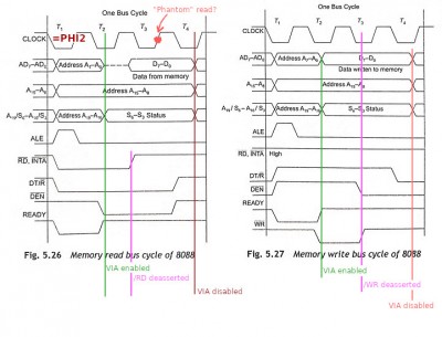
via.jpg
via.jpg [ 88.96 KiB | Viewed 4258 times ]


Now, from W65C22 datasheet:
Quote:
The system PHI2 Input Clock controls all data transfers between the W65C22 and the microprocessor.


Questions:
- Does that mean I cannot read/write VIA without aligning my reads/writes with PHI2?
- As long as VIA is enabled, does it still hold the data bus (during reads) for subsequent PHI2 cycles?
- How exactly does VIA use PHI2 (besides counters)? Does it gate PHI2 with R/W?

Worst case which I think can happen is double reads/writes to/from VIA, which is not critical for me. Are there any hidden caveats that I'm missing?

P. S. I know most 80xx CPUs come with optional controller chips (and there's probably one for I/O as well), but I want to build all the glue logic by myself without resorting to Intel's chips.

EDIT: I think there are more issues on the way, since I don't think VIA will hold data long enough (i. e. for more than 1 PHI2 cycle) for 8088 to sample it.
But once I start adding latches to help 8088 talk to VIA, I'll end up having too much glue logic. I guess I'll have to use a different chip that's not as dependent on clock as VIA.

EDIT 2: I could simply use "/RD AND /WR" as PHI2 input to get correct timings, but then I'll lose VIA's timers.

EDIT 3: Is anyone aware of any alternative parallel I/O chips similar to VIA but not reliant on clock signal - i. e. strobed by /RD & /WR?

_________________
/Andrew

deck65 - 6502 slab with screen and keyboard | ПК-88 - SBC based on KM1810VM88 (Ukrainian i8088 clone) | leo80 - simple Z80 SBC
nice65 - 6502 assembly linter | My parts, footprints & 3D models for KiCad/FreeCAD


Top
 Profile  
Reply with quote  
PostPosted: Sun Sep 24, 2023 9:17 pm 
Offline
User avatar

Joined: Fri Aug 30, 2002 1:09 am
Posts: 8543
Location: Southern California
The asymmetry is not a problem.

The VIA gates or latches everything with Φ2; so even if you keep the register-select, chip-select, and read/write lines unchanged but Φ2 goes down and up a couple of times, that's still two operations.  Even on read operations, it will release the bus when Φ2 is low.  (Bus capacitance will hold the last value for quite a while though, maybe many milliseconds (not just nanoseconds or even microseconds), if nothing else drives the bus and all loads are CMOS.)  See the data sheet for the various status changes that can happen with an access, to see if you'll need to make special accommodations.  What comes to mind right away are interrupt flags, handshaking, and maybe shift-register operations.

_________________
http://WilsonMinesCo.com/ lots of 6502 resources
The "second front page" is http://wilsonminesco.com/links.html .
What's an additional VIA among friends, anyhow?


Top
 Profile  
Reply with quote  
PostPosted: Mon Sep 25, 2023 2:14 am 
Offline
User avatar

Joined: Sun Dec 29, 2002 8:56 pm
Posts: 460
Location: Canada
Could you clock the 6522 from an inverted ALE? Then invert RD and use it for RW. ALE sort of serves the purpose of PHI02.

The issue with using ALE is that it may not have the same period all the time. Depends how accurate a clock is needed for the 6522.

_________________
http://www.finitron.ca


Top
 Profile  
Reply with quote  
PostPosted: Tue Sep 26, 2023 4:35 am 
Offline

Joined: Mon May 21, 2018 8:09 pm
Posts: 1462
Lots of different bus designs can be made to work with "asynchronous" devices like the common parallel-bus SRAMs and EEPROMs with relatively little effort. The VIA is, however, specifically designed to work as a synchronous bus device, and assumes that the bus will be a 65xx bus. This works great when the bus is driven by an actual 6502, 65816, or 6800-family CPU, which all like to complete a bus transaction in a single cycle. However, 80-family CPUs (and the 68K family) always take multiple cycles for a bus transaction. I think this is because they were originally designed around a multiplexed bus, which is a relatively good choice for interfacing with DRAM but falls apart for just about anything else.

My recommendation would be to divide the CPU's master clock to provide the VIA's Phi2 clock. The latter can then be slow enough for the CPU to complete a bus transaction in one VIA clock. If the CPU initiates a bus transaction with the VIA out of phase, you'll need to insert wait-states until it gets back into phase. This has the advantage that the VIA's timers will advance at a consistent rate.

For all dedicated 65xx-bus devices, the address and control signals are latched on Phi2 rising edge, and data is valid (in either direction) on Phi2 falling edge. Those are the constraints you must meet when adjusting the CPU timing.


Top
 Profile  
Reply with quote  
PostPosted: Thu Nov 09, 2023 5:04 pm 
Offline

Joined: Wed Aug 21, 2019 6:10 pm
Posts: 217
What is labelled as the "phantom read" might be targeted as the actual read, if the chip select is qualified on both Ready and Read being High. In the Read cycle, the /WR line used as R/W will be high, so if the VIA is not selected until the rising edge preceding the high Phi2 cycle labelled "phantom read", there is your single phi2=1 read cycle. That qualification will still work for the Write cycle, because /RD is high throughout so it is "as if" it is just qualified on Ready.

I do not know the other bus cycles for the 8088, but I presume they are similar to the Z80 in that they need to be checked to work out what else is needed to qualify the chip select to avoid treating some other bus cycle as a VIA Read. That is /M1 in the Z80 ... I don't what which line or lines it is in the 8088.

A0-A2 for the VIA is latched when the Address Latch Enable is high, which is before the Ready line goes high, but qualifying on /RD=1 as well means that the read has valid data on the Address/Data lines throughout the Phi2=1 clock phase, so set-up times for the data being valid before the falling edge of Phi2 are not a concern.

________________
Rob Finch wrote:
Could you clock the 6522 from an inverted ALE? Then invert RD and use it for RW. ALE sort of serves the purpose of PHI02.

The issue with using ALE is that it may not have the same period all the time. Depends how accurate a clock is needed for the 6522.


If I am reading the timing diagram correctly, the Address Latch Enable is high to indicate that there are Address Bits on AD0-AD7 and on the high Address/Status lines as well. You wouldn't have your data byte available to be read in that T-cycle. It's like if the 65816 had a latch line that went high in the second half of the PHI2=0 phase for latching the bank address.


Top
 Profile  
Reply with quote  
Display posts from previous:  Sort by  
Post new topic Reply to topic  [ 5 posts ] 

All times are UTC


Who is online

Users browsing this forum: No registered users and 18 guests


You cannot post new topics in this forum
You cannot reply to topics in this forum
You cannot edit your posts in this forum
You cannot delete your posts in this forum
You cannot post attachments in this forum

Search for:
Jump to: