6502.org Forum  Projects  Code  Documents  Tools  Forum
It is currently Thu May 09, 2024 10:45 pm

All times are UTC


Post new topic Reply to topic  [ 3 posts ] 
Author Message
PostPosted: Wed Aug 16, 2023 4:54 pm 
Offline
User avatar

Joined: Sat Jun 08, 2013 4:02 pm
Posts: 46
This solution/suggestion is a way to utilize what I already have. Starting from scratch there'd be other ways to achieve the same result, possibly with addresses not so widely spaced.

Back in the day I expanded my VIC20's I/0 space $8000-9FFF into 4K of RAM "under" the Character ROM, a number of 32-location I/O slots, two 16-location slots (one of which was used for a Configuration Register) and 512 bytes of RAM.

If I use the 16-location $915x slot /CS to qualify a Write for a 74_670 and AND that with the 1/2K RAM /CS Writes to the '670 would also write the RAM. The four '670 Write registers also occupy (with repeating images) the first 16 locations of the 1/2K. There'd then be no need to do two Writes, one to the '670 and one to readable RAM so that what was written could later be Read, if needed.
Attachment:
readable_670.gif
readable_670.gif [ 15.46 KiB | Viewed 1765 times ]

Frankly, I don't find the Write twice method especially onerous, but if it can be painlessly eliminated, so much the better.

STA 915x; write a 670 register
; do other stuff
;
LDA 920x; read what was written

_________________
"I am endeavoring, ma'am, to create a mnemonic memory circuit... using stone knives and bearskins." -- Spock to Edith Keeler


Top
 Profile  
Reply with quote  
PostPosted: Thu Aug 17, 2023 4:53 pm 
Online
User avatar

Joined: Fri Dec 11, 2009 3:50 pm
Posts: 3354
Location: Ontario, Canada
Quote:
Writes to the '670 would also write the RAM
I like it! :)

And of course the same sort of arrangement can allow a '573 or '574, used as an output port, to be read back.

Quote:
There'd then be no need to do two Writes, one to the '670 and one to readable RAM so that what was written could later be Read, if needed.
Yup. Additionally, in certain cases it's quite nice to be able to use a Read-Modify-Write instruction to alter what's been previously written.

BTW you haven't explained that your '670 is used as part of a memory mapping scheme... a job for which it is eminently suited!

For anyone who's curious, there's more on the '670 (including memory mapping schemes) here.

-- Jeff

_________________
In 1988 my 65C02 got six new registers and 44 new full-speed instructions!
https://laughtonelectronics.com/Arcana/ ... mmary.html


Top
 Profile  
Reply with quote  
PostPosted: Sat Aug 19, 2023 7:40 pm 
Offline
User avatar

Joined: Sat Jun 08, 2013 4:02 pm
Posts: 46
Dr Jefyll wrote:
BTW you haven't explained that your '670 is used as part of a memory mapping scheme... a job for which it is eminently suited!

With A14 A15 on WA, WB the '670 would provide four bits for each 16K region of a 64K address range. Each of the 4 bits could be "extended" address bits or some combination of address and control, depending on the region. I haven't worked out all the details yet, but I'm striving for something that wouldn't be overkill for a VIC-20, unlike other schemes I've thought up, which were both overkill and extremely pricey! For now I'm just putting out ideas that might be useful or spark suggestions or criticisms.

The 512bytes of RAM in IO space of my earlier mod is intended to be memory that wouldn't be accessed by code not written by me. It could hold short routines for managing my enhancements, or wedges to add or alter Basic operations, etc. I've come up with two other ways to make 74_670 Write registers readable. One is specific my expanded RAM-in-I/O modification, the other is more generalized.

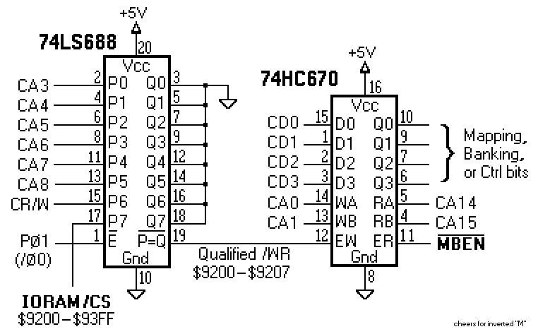
Below, instead of having an IO slot also appear in the small RAM space, accessing locations of that RAM also access the '670 registers. The '670 Read and Write will be at the same addresses, which would be a big improvement over my earlier post.
Attachment:
670+688.GIF
670+688.GIF [ 10.9 KiB | Viewed 1624 times ]

Besides carving out four locations (plus four more as images) for the '670, the '688 also qualifies the raw cpu R/W. (The IO RAM gets VIC's normal VR/W.) It's important to note that until '670 ER goes low its Q outputs will be tristated, presumably pulled up to 1111, which will establish the Mapping/Banking/whatever powerup default state. /MBEN

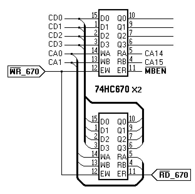
In the circuit below, two '670s are used, one in the expected manner, the 2nd as readback of what was written to the 1st. It's assumed that /WR and /RD specific to the '670s' location have been decoded and qualified.
Attachment:
670x2.GIF
670x2.GIF [ 9.22 KiB | Viewed 1624 times ]

I'm pretty sure I've seen something similar, or possibly exactly like it, elsewhere in this forum.

Another germane thread is here: ram banking
viewtopic.php?f=4&t=7591

(Waiting for the resident '816 devotees to pooh pooh all the above folderol.)

_________________
"I am endeavoring, ma'am, to create a mnemonic memory circuit... using stone knives and bearskins." -- Spock to Edith Keeler


Top
 Profile  
Reply with quote  
Display posts from previous:  Sort by  
Post new topic Reply to topic  [ 3 posts ] 

All times are UTC


Who is online

Users browsing this forum: No registered users and 5 guests


You cannot post new topics in this forum
You cannot reply to topics in this forum
You cannot edit your posts in this forum
You cannot delete your posts in this forum
You cannot post attachments in this forum

Search for:
Jump to: