6502.org Forum  Projects  Code  Documents  Tools  Forum
It is currently Thu May 09, 2024 8:59 pm

All times are UTC


Post new topic Reply to topic  [ 37 posts ]  Go to page Previous  1, 2, 3
Author Message
PostPosted: Sun Sep 17, 2023 6:43 am 
Offline
User avatar

Joined: Wed May 31, 2023 10:46 pm
Posts: 26
Location: Sebastopol, California
Update 2023-09-16: Keyboard hacked, NVRAM backup, Planning soldered breadboard, Potential fanout issues, Improved clock module

Keyboard hacked:

To avoid using USB and any associated CPUs, and to get lower keypress latencies and better overall control of the keyboard access, I’ve bypassed the KB120 onboard controller and connected wires directly to the keyboard contact matrix. This matrix is formed out of two clear plastic sheets that are each made into a kind of circuit board with silvery traces, but can’t be soldered at any temperature significantly above room temperature. I used the original controller board just to get the connector fingers. Unfortunately these are covered in black, evidently carbon-rich gunk that is hard to get off. After a lot of scraping and using Q-Tips with 91% isopropyl alcohol, I was able to solder hookup wire to the original pads and put them into the crimping system that the keyboard came with. Here is the result, with the keyboard all put back together:
Attachment:
File comment: Keyboard KB120 hacked to get direct connections to the contact matrix
LRC-keyboard-hacked-matrix-lines.jpg
LRC-keyboard-hacked-matrix-lines.jpg [ 3.83 MiB | Viewed 2467 times ]

So far, my spot checks on the matrix connections with a ohm meter indicates this was successful, and I should be able to make a controller/scanner circuit to detect and record keypresses to send to the CPU later.

NVRAM backup:

Earlier in this thread was the suggestion to make backups of the NVRAM that I am working hard to put code into and do laborious font editing. Since the system with NVRAM can be easily corrupted by the CPU running amok (for hardware or software reasons), backups seemed like a priority now.

The module I came up with is ridiculously simple, just two 74F chips, plus a bunch of clock lines from the clock module, a pushbutton switch and a pull-up resistor, plus two sets of five bank-select switches with associated pull-up resistors. The chips are a 74F174 quad flip-flop, and an OR gate. These are used to form the WE\ pulse and CS\ signal on the NVRAM being written. The NVRAM being read from just has all its control lines hooked to +5 or ground as appropriate. Here is the resulting module:
Attachment:
File comment: NVRAM backup copier module
LRC-NVRAM-backup-copier-module.jpg
LRC-NVRAM-backup-copier-module.jpg [ 1.92 MiB | Viewed 2467 times ]

I’ve used this and spot checked the resulting copy. Each NVRAM has 32 banks of 64k each. I also managed to correctly solder three out of five of the NVRAM surface mount chips to the adapter boards. Two of the five were damaged, with certain bits pinned high. I’m glad I splurged to buy a hot air rework station and stencil/squeegee things to apply solder paste to the wee little surface mount pads.

Planning soldered breadboard

Since the proliferation of solderless breadboards was getting out of hand and started to be very finicky to keep going, I’ve decided to make a soldered version of the CPU+video modules, plus some generic memory-mapped I/O parts of the font editor module. My self-designed generic breadboards support only three rows of chips if you don’t cut traces, but I realized that by cutting some traces like you would with stripboards, I could pack six rows of chips onto the breadboard. The tricky thing is to optimize/arrange the layout of the chips and trace cuts to support all the wire connections needed. Here is a diagram I started working on to do this:
Attachment:
File comment: Soldered locker-room-challenge initial board layout puzzle
LRC-soldered-layout1-20230915.jpg
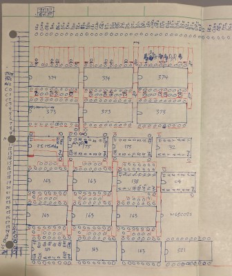
LRC-soldered-layout1-20230915.jpg [ 2.24 MiB | Viewed 2467 times ]

The red lines are where the trace cuts (or edge of the board) would go. Note that I’ve put space between chips that can act as wire fanout enhancers for high-fanout lines like some important clock lines. Anyway, this is an interesting puzzle to work out. Here is what the layout looks like when I put sockets, unsoldered for now, into the breadboard to see how things would work out of what issues might arise:
Attachment:
File comment: LRC actual breadboard testing initial layout
LRC-soldered-layout1-checking-it-out.jpg
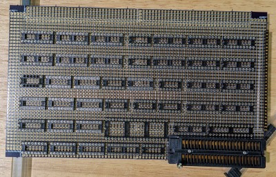
LRC-soldered-layout1-checking-it-out.jpg [ 1.39 MiB | Viewed 2467 times ]

The ZIF socket for the NVRAM is a real beast, pushing things away and causing layout grief. It is also very high profile, as is the NVRAM on its adapter board, so any module stacked on top of these will need a cutout in that corner.

Potential fanout issues

I hadn’t really been thinking about fanouts being an issue, as generally a decent logic family like 74F has something like 30+ fanout if you stick with the same family. However, as I was planning my soldered LCU (Locked Room Challenge) SBC, and adding lots of bytes of latched+buffered memory-mapped I/O, I started to worry about fanout with respect to the W65C02S CPU. Looking at the data sheet I was horrified to see that the CPU can only be expected to drive 1.6 mA (the Iol max rating), which is able to output to less than three 74F inputs! Yikes! I’ve seem some mention on the forums that this part of the WDC data sheet is extremely conservative, but I don’t want to design into dicey territory. So I’m planning to latch the address and data lines on CPU write, and from there write to a bunch of output latches. I will actually reuse the three 74F374 latches I am currently using for the CPU-to-video-ram write, and have that be used for both memory-mapped output generally as well as video ram writing.

In any case, this has caused me to rethink my design to make other improvements I’ve been thinking about. Back to my first module, the power-of-two clocks bank, I’ve found it messy and potentially limiting to have my higher frequency clocks asynchronous from each other (25 12.6 and 6.3 MHz don’t line up with each other). Solution below.

Improved clock module

So to get 25.175 MHz and all divisions by two from that to line up, it helps to have a 50.35 MHz clock to drive these. I have not seen this specific frequency of oscillator module for sale, so I decided to make my own by making a frequency-doubling circuit for my 25.175 MHz clock signal. There are a large number of ways to do this, including some fast analog filtering and rectification bridges, but the simplest seems to be to add a delay line chip to get a ¼ cycle delay and XOR gate inputting the original and delayed clock signal. Initially I just used three 74F04 inverters in series for an appropriate delay, and it worked, but this is really fragile in several ways, and not reliably repeated on a second build or tolerant of parts swaps or temperature changes etc. So I’ve put to use the Maxim DS1100Z-20+ silicon delay line module, that has five taps at multiples of 4ns delay. I use tap 3, nominally 12ns, since that seemed to give a slightly better 50MHz signal with the limited visualizations I could do on my cheap scope. I suppose I could have put in an automated duty cycle optimization circuit based on averaging the clock signal over a long (1000’s of cycles) time window, and comparing to an ideal voltage, but I just want to move on for now.

In addition, I wanted to improve so that all my highest frequency signals have symmetric inverted variants. So I designed my own “enhanced” `163 counter-like circuit using 74F175 quad flip flops and various supporting gates. The flip-flops output symmetric inverted/non-inverted pairs.

Also, since I am clocking all my counters at a *much* higher 50MHz, I went with the fast `163 circuit design, separating the high-frequency part of the carry look-ahead to the ENP pins on the counters all connected together, and the propagation-delay low-frequency chain on RCO-ENT-RCO-ENT-... Here is the overall schematic (LRC appropriate – no computers used!):
Attachment:
File comment: LRC improved clock module schematic
LRC-clock-module-improved-schematic-20230916.jpg
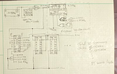
LRC-clock-module-improved-schematic-20230916.jpg [ 540.85 KiB | Viewed 2467 times ]

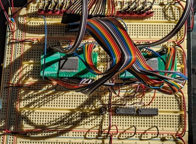
Overall this works great, and I have 32 synchronous power-of-two clock signals going from 25.175 MHz down to a cycle time of around 85 seconds. I believe this will help make for a simpler design and timing analysis process, and hopefully more reliable designs at the end. Here is the prototyped module in action:
Attachment:
File comment: LRC improved clock module in action
LRC-improved-clock-module-in-action.jpg
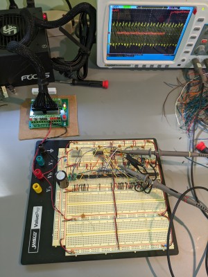
LRC-improved-clock-module-in-action.jpg [ 7.51 MiB | Viewed 2467 times ]

My next steps are to work out the revised LRC SBC design with the fanout from the CPU minimized, redo the layout once that is done, and start soldering.

_________________
--Mark


Top
 Profile  
Reply with quote  
PostPosted: Sun Sep 17, 2023 9:53 am 
Offline

Joined: Fri Jul 09, 2021 10:12 pm
Posts: 741
Nice update, that keyboard must have been frustrating - I don't like soldering things that don't want to be soldered!

The counter solution is good too, it sounds like you're building a solid foundation there. I like the 175 with its inverted outputs and common clock. I think you mislabelled some of the frequencies in that part of your schematic though, especially the top half of the chip!


Top
 Profile  
Reply with quote  
PostPosted: Sun Sep 17, 2023 2:23 pm 
Offline
User avatar

Joined: Fri Dec 11, 2009 3:50 pm
Posts: 3354
Location: Ontario, Canada
Quote:
So I’m planning to latch the address and data lines on CPU write, and from there write to a bunch of output latches.
Sounds like a non-trivial alteration. :|

Would you bother with all this extra work if the fanout issue were magically solved? Because I suspect it easily can be, if you'll just swap out most or all of those creepy 74F series chips!

The inputs of CMOS families such as AC, AHC, LV and others (including the related "T" variants) have essentially zero DC loading, making fanout unlimited in that regard. At some point (>10 inputs driven?) you do begin to need to pay attention to the AC consideration of input capacitance, but that issue is a great deal less limiting than the DC constraint.

The 74F Series is a bit of a dinosaur, IMO. Its speed is the only thing it has going for it. The power consumption is high, and it supplies only TTL output levels. In some cases TTL output levels are more or less OK, but when driving WDC CPU inputs they're asking for trouble. 74F input levels are also TTL, which means noise immunity is inferior to the CMOS families I mentioned (other than the T variants, of course). More on logic levels and WDC here.

74AHC/AHCT is probably the most forgiving option to work with. 74AC/ACT might be a bit faster, but its outputs -- like those on WDC CPU's -- have aggressively fast rise and fall times. (And 74F probably isn't much better, although I admit I haven't checked.)

-- Jeff

_________________
In 1988 my 65C02 got six new registers and 44 new full-speed instructions!
https://laughtonelectronics.com/Arcana/ ... mmary.html


Top
 Profile  
Reply with quote  
PostPosted: Sun Sep 17, 2023 3:54 pm 
Offline
User avatar

Joined: Wed May 31, 2023 10:46 pm
Posts: 26
Location: Sebastopol, California
Dr Jefyll wrote:
Quote:
So I’m planning to latch the address and data lines on CPU write, and from there write to a bunch of output latches.
Sounds like a non-trivial alteration. :|

Would you bother with all this extra work if the fanout issue were magically solved? Because I suspect it easily can be, if you'll just swap out most or all of those creepy 74F series chips!

The inputs of CMOS families such as AC, AHC, LV and others (including the related "T" variants) have essentially zero DC loading, making fanout unlimited in that regard. At some point (>10 inputs driven?) you do begin to need to pay attention to the AC consideration of input capacitance, but that issue is a great deal less limiting than the DC constraint.

The 74F Series is a bit of a dinosaur, IMO. Its speed is the only thing it has going for it. The power consumption is high, and it supplies only TTL output levels. In some cases TTL output levels are more or less OK, but when driving WDC CPU inputs they're asking for trouble. 74F input levels are also TTL, which means noise immunity is inferior to the CMOS families I mentioned (other than the T variants, of course). More on logic levels and WDC here.

74AHC/AHCT is probably the most forgiving option to work with. 74AC/ACT might be a bit faster, but its outputs -- like those on WDC CPU's -- have aggressively fast rise and fall times. (And 74F probably isn't much better, although I admit I haven't checked.)

-- Jeff


Thanks Jeff for the heads up on W65C02S input levels not being quite TTL compatible! Nice write-up that I will dig into.

I did spend a bit of time settling on 74F, and some of the main pluses are speed and availability of a wide variety of parts, plus easier prototyping with through-hole pins available. For example, you can get 74F21 (dual 4-input AND)
or 74F175 (quad flip flop) but thereare no 74AHCT equivalents available. I'd be super happy to have something like the super fast CMOS families if I could get enough diversity of parts and through-hole pins and no weird level translations talking to the W65C02S running at 5v. I didn't want the hassle of figuring out which 74 series to use for which function, and instead just keep everything in the same family for the most part. Eventually, when I either get out of "locked room challenge" mode or get to a point where I can bootstrap myself to a certain level, I might switch to CPLDs for the speed and reduction of chip count.

Through-hole pins are a big win on rapid prototyping for me -- it is a tedious, long, and error-prone process for me to solder the teeny little SMDs to adapter boards.

Also, I'm already using `374s to latch the CPU address and data on video RAM write -- I'm just going to expand the use of those same three chips to capture all writes and go from there to both video RAM and to the bank of memory-mapped output latches, and even put those onto the expansion bus pins. So mainly a bit of control logic changes, in some cases making things a bit simpler, in some cases a bit more complex. The only downside is a bit of increased latency in writing to the memory-mapped output latches, but I don't think that matters for any practical purpose I can think of now.

_________________
--Mark


Top
 Profile  
Reply with quote  
PostPosted: Mon Sep 18, 2023 2:53 am 
Offline
User avatar

Joined: Fri Dec 11, 2009 3:50 pm
Posts: 3354
Location: Ontario, Canada
Alright, Mark... I do understand and sympathize with your position. And I didn't mean to come across as though I expected you to re-engineer the whole project all at once.

But some piecemeal changes may bear consideration, particularly in regard to signals that need to get input by the CPU. Much as you may prefer to avoid mixing logic families, you *are* in effect doing so as long as your recipe includes both 74F series and that WDC CPU. :!:

One solution would be to swap out the WDC CPU and put in a non-WDC 'C02 such as Rockwell, as the latter has inputs that do respond reliably to the TTL levels output by 74LS, ALS, F etc.

The alternative solution is to use a CMOS logic family such as HC, HCT, AC, ACT, AHC, AHCT etc for any chip whose output needs to feed an input on the WDC.

And it really isn't that much hassle to get up to speed on the various families. Where simple logic chips such as gates and flipflops are concerned (as opposed to memory and LSI), we can summarize the issue of voltage levels as follows (and I'll assume all the chips are powered by 5V, as in your project): There are just three basic categories. For reliable operation, ...

    - HC, AC, AHC etc require a full voltage swing at their inputs. They provide a full voltage swing at their outputs.
    - HCT, ACT, AHCT etc can accept the smaller TTL voltage swing at their inputs. They provide a full voltage swing at their outputs.
    - LS, ALS, F etc can accept the smaller TTL voltage swing at their inputs. They provide only the smaller TTL voltage swing at their outputs.

A WDC 'C02 has the characteristics of the first category. A Rockwell or other non-WDC 'C02 has the characteristics of the second category.

-- Jeff

_________________
In 1988 my 65C02 got six new registers and 44 new full-speed instructions!
https://laughtonelectronics.com/Arcana/ ... mmary.html


Top
 Profile  
Reply with quote  
PostPosted: Mon Sep 18, 2023 4:32 am 
Offline
User avatar

Joined: Wed May 31, 2023 10:46 pm
Posts: 26
Location: Sebastopol, California
gfoot wrote:
Nice update, that keyboard must have been frustrating - I don't like soldering things that don't want to be soldered!

The counter solution is good too, it sounds like you're building a solid foundation there. I like the 175 with its inverted outputs and common clock. I think you mislabelled some of the frequencies in that part of your schematic though, especially the top half of the chip!


D'Oh! I did mislabel those frequencies, and the schematic was a bit too messy, so I've made a (hopefully) better version:
Attachment:
File comment: LRC improved clock module schematic, take 2
LRC-improved-clock-module-schematic-v2.jpg
LRC-improved-clock-module-schematic-v2.jpg [ 1.57 MiB | Viewed 2254 times ]


On the keyboard mod messiness, someone posted a nice little custom board that replaces the original and has the pads/fingers on the edge to make contact with the keyboard matrix sheets. I did not want to go that far for now and just did the more hacky thing.

_________________
--Mark


Top
 Profile  
Reply with quote  
PostPosted: Mon Sep 18, 2023 5:23 am 
Offline
User avatar

Joined: Wed May 31, 2023 10:46 pm
Posts: 26
Location: Sebastopol, California
Dr Jefyll wrote:
Alright, Mark... I do understand and sympathize with your position. And I didn't mean to come across as though I expected you to re-engineer the whole project all at once.

But some piecemeal changes may bear consideration, particularly in regard to signals that need to get input by the CPU. Much as you may prefer to avoid mixing logic families, you *are* in effect doing so as long as your recipe includes both 74F series and that WDC CPU. :!:

One solution would be to swap out the WDC CPU and put in a non-WDC 'C02 such as Rockwell, as the latter has inputs that do respond reliably to the TTL levels output by 74LS, ALS, F etc.

The alternative solution is to use a CMOS logic family such as HC, HCT, AC, ACT, AHC, AHCT etc for any chip whose output needs to feed an input on the WDC.

And it really isn't that much hassle to get up to speed on the various families. Where simple logic chips such as gates and flipflops are concerned (as opposed to memory and LSI), we can summarize the issue of voltage levels as follows (and I'll assume all the chips are powered by 5V, as in your project): There are just three basic categories. For reliable operation, ...

    - HC, AC, AHC etc require a full voltage swing at their inputs. They provide a full voltage swing at their outputs.
    - HCT, ACT, AHCT etc can accept the smaller TTL voltage swing at their inputs. They provide a full voltage swing at their outputs.
    - LS, ALS, F etc can accept the smaller TTL voltage swing at their inputs. They provide only the smaller TTL voltage swing at their outputs.

A WDC 'C02 has the characteristics of the first category. A Rockwell or other non-WDC 'C02 has the characteristics of the second category.

-- Jeff


Thanks Jeff, indeed the main chips outside the NVRAM that output to the W65C02S are `373s in the updated design I'm working on, and it looks like 74AHCT373 is similar in speed to the 74F373. So I think I will order some of those for that specific purpose. In general though 74AHCT seems slower and has less through-hole parts available than 74F, so I'll stick with the F's for the rest for now. I'm not inputting a lot of control signals into the CPU, but there is phi2 and reset in my case. Reset is not a big deal, but phi2 I really want to keep synced with all my other clocks, and unfortunately I don't see a 74AHCT175 available, and the 74HCT175 is way too slow. There is a 74ABT octal flip flop that seems interesting, but it doesn't have the symmetric inverted/non-inverted outputs. Also, my clock lines go all over the place, so if I change those outputs to a lower Iol family, that forces me to move away from 74F just about everywhere. Is there some super low-latency (say < 2ns) way to level shift the phi2 input to the CPU while running at 12.5875 MHz while keeping the CPU at 5v? Something like SN74LVC1T45, if I'm reading the data sheet correctly, can do the translation in around 7ns max, but that is too slow for my purposes. Hmm, looking around I see 74ABT74, but some of the specs like max input rise rate seem scary...I'll need to keep looking.

[Edit: Okay, looks like I can use a 74AHCT74 flip flop running in parallel with the 74F175 for the high frequency counting for the 25.175 MHz and 12.5875 MHz clocks, and the propagation delays are maybe within 2ns of each other, but it will require the one extra chip.]

_________________
--Mark


Top
 Profile  
Reply with quote  
Display posts from previous:  Sort by  
Post new topic Reply to topic  [ 37 posts ]  Go to page Previous  1, 2, 3

All times are UTC


Who is online

Users browsing this forum: No registered users and 12 guests


You cannot post new topics in this forum
You cannot reply to topics in this forum
You cannot edit your posts in this forum
You cannot delete your posts in this forum
You cannot post attachments in this forum

Search for:
Jump to: