6502.org Forum  Projects  Code  Documents  Tools  Forum
It is currently Sat Apr 27, 2024 5:42 pm

All times are UTC


Post new topic Reply to topic  [ 111 posts ]  Go to page Previous  1, 2, 3, 4, 5 ... 8  Next
Author Message
PostPosted: Tue Jul 18, 2023 3:01 am 
Offline

Joined: Fri Jul 09, 2021 10:12 pm
Posts: 741
BigDumbDinosaur wrote:
I don’t see a memory map posted anywhere. Kind of hard to decipher a new design without one.

At the moment there's just 32K of RAM from $0000-$7FFF, and anything with A15 set is ROM or I/O - that's going to be decoded outside of this core circuit, on the I/O module. The most appealing option so far is a PLD in the I/O module that decodes $8000-$FF00 as ROM, with the region above that being split between ROM and I/O devices so that at least the vectors come from ROM. I'm not too concerned about finalising that as it's up to the PLD - any reasonable arrangement with at least 32-byte granularity should work I think.


Top
 Profile  
Reply with quote  
PostPosted: Tue Jul 18, 2023 7:52 am 
Offline
User avatar

Joined: Sat Jul 24, 2021 1:37 pm
Posts: 282
Looks great to me!

I would maybe use AHC(T) transceivers, and an AHC(T) flip flop for even more speed.

You should know that since recently 4 layers boards are cheap until 100x100 (6€)

_________________
BB816 Computer YouTube series


Top
 Profile  
Reply with quote  
PostPosted: Tue Jul 18, 2023 2:14 pm 
Offline
User avatar

Joined: Fri Dec 11, 2009 3:50 pm
Posts: 3346
Location: Ontario, Canada
Based on a quick look, there's one point that jumps out at me. It's great that you're keeping the ROM and IO isolated from the RAM/CPU core. This'll allow the latter to achieve higher speeds. But allow me to suggest a slight but important change to the glue logic.

The 'C02 makes no use of the data bus while Phi2 is low, so there's no benefit to having the bus driven. In fact, there's a solid advantage to NOT driving the bus while Phi2 is low, because that 50% "dead time" provides a wonderful timing cushion when the bus gets handed off from one device to another.

Your original glue logic keeps the data-bus transceiver continuously enabled, thus squandering the benefit of the timing cushion and putting you at risk of several nanoseconds of bus contention just as one device stops driving the bus and another devices starts. This is "tolerable" in the limited sense that it probably won't cause a gross error such as crashing the machine. However, the fraction of a cycle of bus contention injects noise into the bus lines and the power supply, thus eroding your goal of a quiet and fast machine.

Here's a suggested revision that restores the timing cushion. I added an inverter, but it won't be required if you swap the A and B buses on the transceiver.

-- Jeff


Attachments:
6502fastpdipschematic2 (JL edit).png
6502fastpdipschematic2 (JL edit).png [ 40.22 KiB | Viewed 26082 times ]

_________________
In 1988 my 65C02 got six new registers and 44 new full-speed instructions!
https://laughtonelectronics.com/Arcana/ ... mmary.html
Top
 Profile  
Reply with quote  
PostPosted: Tue Jul 18, 2023 4:22 pm 
Offline

Joined: Fri Jul 09, 2021 10:12 pm
Posts: 741
Dr Jefyll wrote:
Here's a suggested revision that restores the timing cushion. I added an inverter, but it won't be required if you swap the A and B buses on the transceiver

Thanks Jeff. I do however need the transceiver enabled even when PHI2 is low if RDY is also low, at least for write operations, as slower devices will be expecting XD[0..7] to remain stable for a longer period. I could either do as you suggest but only for read cycles, or possibly just add a latch after the transceiver to hold the value for the duration of the write operation. The latter is quite easy, and leads towards the possibility of overlapping I/O writes with RAM-based cycles - so an I/O write operation wouldn't require any wait states unless another I/O operation follows before the write is complete.

akohlbecker wrote:
I would maybe use AHC(T) transceivers, and an AHC(T) flip flop for even more speed.

You should know that since recently 4 layers boards are cheap until 100x100 (6€)

Hmm I'll have to recheck the board prices! The speeds of the transceivers and flipflop are probably not critical as they mostly drive the I/O module, which is slow. So long as the flipflop is quick enough to pull RDY low within the PHI2 duration I think it should be OK - I can try a faster one though if that's not working.


Top
 Profile  
Reply with quote  
PostPosted: Tue Jul 18, 2023 10:12 pm 
Offline
User avatar

Joined: Fri Dec 11, 2009 3:50 pm
Posts: 3346
Location: Ontario, Canada
gfoot wrote:
I do however need the transceiver enabled even when PHI2 is low if RDY is also low, at least for write operations, as slower devices will be expecting XD[0..7] to remain stable for a longer period.
Thanks for drawing my attention to that point, one I hadn't considered in detail until now. At issue is the interval from the end of the Phi2-high period of the initial CPU write cycle (the RDY-low, "wait state" cycle) until the beginning of the Phi2-high period of the subsequent cycle.

It's plausible that capacitance on the XD[0..7] bus lines will be enough to keep them stable during said interval. But of course merely being stable isn't enough -- we need them to be stable at valid logic levels! So, will the XD bus lines have reached valid logic levels by the end of the Phi2-high period of the initial CPU write cycle?

I don't see a problem, provided that the XD bus isn't physically very long and that it isn't connected to too much capacitance (say, ten or more device inputs). And BTW I echo the suggestion to consider changing that transceiver from an HC type to AHCT... "A" for the reduced prop delay, and "T" to accommodate the possibility that there are devices on the XD bus which output only TTL levels, not CMOS levels.


Quote:
I could either do as you suggest but only for read cycles, or possibly just add a latch after the transceiver to hold the value for the duration of the write operation. The latter is quite easy, and leads towards the possibility of overlapping I/O writes with RAM-based cycles - so an I/O write operation wouldn't require any wait states unless another I/O operation follows before the write is complete.
Well, FWIW, this whole "stable data" issue goes away if you forget using RDY and opt for clock stretching instead. And, hm, intriguing idea about overlapping I/O and RAM cycles, but it sounds as if you'd need to latch the address too, not just the data...

-- Jeff

_________________
In 1988 my 65C02 got six new registers and 44 new full-speed instructions!
https://laughtonelectronics.com/Arcana/ ... mmary.html


Top
 Profile  
Reply with quote  
PostPosted: Wed Jul 19, 2023 12:42 am 
Offline

Joined: Fri Jul 09, 2021 10:12 pm
Posts: 741
Dr Jefyll wrote:
It's plausible that capacitance on the XD[0..7] bus lines will be enough to keep them stable during said interval. But of course merely being stable isn't enough -- we need them to be stable at valid logic levels! So, will the XD bus lines have reached valid logic levels by the end of the Phi2-high period of the initial CPU write cycle?

I don't see a problem, provided that the XD bus isn't physically very long and that it isn't connected to too much capacitance (say, ten or more device inputs).

Ten is pushing it, but my I/O PLD can support six devices plus ROM, so I guess it is heading in that direction. I am generally trying to assume that the X buses are much more badly loaded, and not put constraints on that. It's plausible for example that I/O modules could be separate boards, or something similar to the ISA bus in early PCs. I *think* the wait state system would tolerate really slow I/O, and for example a device at the other end of a ribbon cable might be OK so long as IOWAIT and IOREADY aren't faster to arrive than the X bus signals. Obviously this isn't my first concern, but it does feel potentially possible.

Quote:
And BTW I echo the suggestion to consider changing that transceiver from an HC type to AHCT... "A" for the reduced prop delay, and "T" to accommodate the possibility that there are devices on the XD bus which output only TTL levels, not CMOS levels.

I have plenty of AHCT transceivers and flip-flops, as I use them in my VGA circuits when the bus switches mode back and forth twice per clock cycle, so I can certainly use those if necessary.

Quote:
Well, FWIW, this whole "stable data" issue goes away if you forget using RDY and opt for clock stretching instead.

I saw your clock stretching using a '163 idea. I could possibly also consider using a multiplexer to switch between copying the oscillator output and outputting a constant high level, based on the current IOWAIT/RDY state. I haven't thought of any downsides to clock stretching.

Quote:
And, hm, intriguing idea about overlapping I/O and RAM cycles, but it sounds as if you'd need to latch the address too, not just the data...

This was my first paper sketch of the project...
Attachment:
20230715_184649.jpg
20230715_184649.jpg [ 3.41 MiB | Viewed 26029 times ]

... and this is why they changed to transceivers:
Attachment:
20230715_184707.jpg
20230715_184707.jpg [ 2.3 MiB | Viewed 26029 times ]

i.e. loading the RAM from ROM during reset. The current circuit is not capable of that yet, so is a bit of a middle ground!


Top
 Profile  
Reply with quote  
PostPosted: Wed Jul 19, 2023 12:54 pm 
Offline

Joined: Fri Jul 09, 2021 10:12 pm
Posts: 741
I wasn't going to think too much about the I/O module side of things in a first pass, as I thought I'd see about getting the core actually working first - but since I backtracked on the initial prototype circuit and added the I/O module anyway, I thought I'd share the current plan for that, and also some thoughts on getting 6522 VIAs to work with a clock that's independent of the core system.

Apologies for the length, there are quite a lot of elements here, it may be interesting for some people though!

So this is the current I/O module schematic, containing a PLD to drive things, some ROM to boot from, and a simple output port:

Attachment:
iomodule1.png
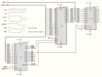
iomodule1.png [ 46.57 KiB | Viewed 25993 times ]


XA[0..15] and XD[0..7] are the buffered address and data lines; XRWB is a buffered copy of RWB; and IOWAIT is as in the earlier circuits, and also discussed in more detail below.

The waveforms illustrate roughly what's meant to happen. PHI2 is the core system clock, and A15 is the CPU's A15 pin. If this is low, the access is from RAM and dealt with by the core system I posted above; if A15 is high then it's some form of slow operation, either ROM or I/O, and the core system sets IOWAIT high if this is the case on a rising edge of PHI2. The inverse of this forms the RDY signal to the CPU. (But note that I am still considering clock stretching, and am perhaps likely to replace the RDY mechanism with one that holds the CPU's PHI2 pin high directly rather than using RDY - the general mechanism and timing of this phase will be pretty much the same.)

That condition then persists until the I/O module asserts ~IOREADY low - the core system samples this on the rising edge of PHI2 and, if it's low, then IOWAIT is reset, allowing RDY to go high and the CPU to continue its processing. The I/O module can wait as long as it needs to before doing this; and the I/O module must reset ~IOREADY to the high state whenever IOWAIT is not active, as ~IOREADY is level-triggered. (This isn't illustrated correctly in the waveform diagram.)

The lower three waveforms illustrate the I/O module's response - ~IOREADY will stay high for a while and then go low; and it also synthesizes the ~IOOE and ~IOWE signals depending on the state of RWB. I've shown ~IOOE lasting for the duration of A15 being high - hence at least until the end of the CPU's PHI2 phase, as the CPU would require the data to be driven to the bus for at least that period; but in practice, more and more, I think the data being read needs to actually be latched at the point ~IOREADY goes low, so that individual I/O subsystems don't all need to worry about this. So most likely, ~IOOE will only be asserted while IOWAIT is high - as is already the case there for ~IOWE.

The PLD also outputs chip-select signals for the ROM and various I/O devices. These could be based purely on decoding XA[5..15] but I'm thinking now that at least for the I/O devices I might want to constrain these as well to the period when IOWAIT is high - I'll explain that a bit when I come to VIA interfacing. It is taken as a given that all the devices here are relatively slow, they will always incur at least one wait state, so there's no harm in them taking a short while to activate after IOWAIT goes high - it certainly won't lead to instability for example, as everything is going to stop and wait for them anyway.

Here ~IO0 is tentatively wired through to a latch for debugging purposes - that's obviously not a great solution, it will activate during read accesses as well as write accesses, but it may be minimally sufficient to get at least some output from the system. ~IOWE is fully-qualified by IOWAIT, so the XA address will be valid throughout, and the XD data should be valid soon after IOWAIT goes high (at least before the end of the first PHI2 cycle) and then continuously at least until IOWAIT goes low again, as RDY would have been pausing the CPU during this period. (I hope I've understood the RDY mechanism correctly in that respect.)

--- VIA interfacing ---

So then, regarding VIA interfacing, these need more than just ~CS, ~OE and ~WE, as they need a consistent clock, and they can only read or write data at particular points during their clock cycle. In the BBC Micro the clock used by the VIA and other slow devices is simply half the speed of the main CPU clock, and the system carefully stretches the high portion of the CPU clock - and the low portion as necessary - to get it in sync for just one clock cycle, when accessing a slow device.

I think I would prefer to just let the VIA have its own independent clock without forcing any particular relationship to the CPU clock. Especially if I want to vary the CPU clock quite freely, I don't want to have to change clock divisors to keep the VIA stable in the meantime. So I'll use a separate VIACLK signal, maybe at 1MHz or 4MHz or something like that. This will be ticking away all the time, and the VIA will be using it to control its background operations like decrementing timers and shifting the shift register.

When the CPU wants to read or write a VIA register, it is important that we coordinate the VIA's chip-select and RWB signals carefully. It needs both to be set up while its clock is low, and a certain amount in advance of its clock going high. It's especially important that we don't let its chip-select randomly activate while the CPU's address bus is unstable, as this could be happening while the VIA's clock is high or near its edge. We also must only hold its chip-select high for one of its clock cycles - we don't want two rising clock edges during this period.

So the relationship between the various signals should look something like this:

Attachment:
20230719_095544.jpg
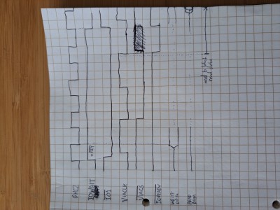
20230719_095544.jpg [ 4.7 MiB | Viewed 25992 times ]


PHI2 is the core CPU clock, and IOWAIT and ~IO1 are as discussed above. VIACLK is the VIA's local clock, and ~VIACS is its active-low chip-select signal. ~IOREADY is as discussed above - we need to bring it low when we're ready for the CPU to unpause. I also sketched in the periods where the XD data bus has valid data from the CPU for writing, and when it needs to have valid data for the CPU to read (unfortunately almost off the right hand edge of the diagram). This does imply I need to latch the data from the VIA for the CPU to read, as the VIA itself won't hold the data valid for very long after its clock falls. As I mentioned earlier, I think latching this when ~IOREADY falls is probably a good option, so that the VIA I/O submodule's only responsibility is driving ~IOREADY low at whatever time it needs.

And here's the circuit I sketched to do some/all of this - it was just a sketch of how it could work, but with the correction I made there, I think it might be OK.

Attachment:
20230719_095531.jpg
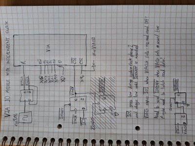
20230719_095531.jpg [ 4.76 MiB | Viewed 25992 times ]


The flipflop that generates ~VIACS is driven by the VIA's clock's falling edge, to try to get half a clock cycle of setup time before the VIA sees the next rising edge. This is a more than is needed and might even be too close to the clock's falling edge, I haven't checked the datasheets. It may be necessary to use a faster crystal divided down to form VIACLK, and synchronise some of these things from intermediate points in the clock cycle.

As we are essentially synchronizing signals between two different clock domains, I do wonder about metastability. The extent of my understanding on metastability is that there's a risk that a signal being sampled e.g. by a flipflop will not meet the setup time requirements for the flipflop, and this can lead to unobvious behaviours like extremely slow slew rates or ringing in the flipflop, which components like the VIA might not like. And my understanding is that practical solutions for this are never 100% perfect, but it's generally accepted that having two flipflops in a row gives good enough results - I guess the theory being that if the setup requirements for the first flipflop are not met, at least it will sort its outputs out with enough time to spare before the second flipflop samples them, meaning anything after the second flipflop sees a nice clean fast edge in sync with the local clock. So I believe I should probably add another flipflop there, either triggered by the rising or falling edge of VIACLK, to guard against metastability. If you guys have better references or advice on this than the ones I've found before, I'd love to hear them!

Finally the extra flipflops at the very bottom of the page are responsible for setting ~IOREADY low at the right time. We need to wait for the next falling edge of VIACLK after ~VIACS is asserted, and at that point set ~IOREADY low. This flipflop is then reset to the high state by IOWAIT going low about one PHI2 cycle later, so that ~IOREADY is again unasserted and ready for the next I/O cycle.

I also drew ~VIACS's flipflop getting set by ~IOREADY being low, meaning that once we've found the next falling edge of VIACLK, we turn off ~VIACS so that it doesn't stay low for another rising edge of VIACLK.

So that's roughly what I have in mind at the moment - rather a lot I'm afraid, so thanks if you stuck with me this long! It is very provisional, I wasn't really planning to sort this out in detail yet, but it feels like a good plan I think and I might put the footprints on the PCB at least, and only populate them to test it if the basic system already works OK. Subject to any feedback, of course!

It also strikes me that Andre has probably dealt with this in his old computer, so I'll go and check his schematics again to see!


Top
 Profile  
Reply with quote  
PostPosted: Wed Jul 19, 2023 5:59 pm 
Offline
User avatar

Joined: Sat Jul 24, 2021 1:37 pm
Posts: 282
Funny, I've been designing a circuit very similar to your VIA idea last week, following my thread on RDY. I did not have the concern of another clock domain, but I made detailed timing diagrams to verify that I was able to latch data shown by the VIA and only activate it a single cycle out of many when RDY is low. I did not finish the writing part yet, though. Let me see if I can find some time to share the reading part before the week end.

_________________
BB816 Computer YouTube series


Top
 Profile  
Reply with quote  
PostPosted: Wed Jul 19, 2023 6:14 pm 
Offline
User avatar

Joined: Thu Dec 11, 2008 1:28 pm
Posts: 10793
Location: England
> having two flipflops in a row gives good enough results
That's my understanding too, with the caveat that one might select flops for this purpose which have particularly good behaviour - short setup and hold constraints, and high gain. Also, comparing the MTBF with the operating frequency (and the sales volume) tells you how many billions of operations should succeed for each failure, and in some cases a chain of three flops will be the right answer. For hobby purposes, two is enough (and one might be OK.)


Top
 Profile  
Reply with quote  
PostPosted: Thu Jul 20, 2023 8:48 am 
Offline

Joined: Fri Jul 09, 2021 10:12 pm
Posts: 741
akohlbecker wrote:
Funny, I've been designing a circuit very similar to your VIA idea last week, following my thread on RDY. I did not have the concern of another clock domain, but I made detailed timing diagrams to verify that I was able to latch data shown by the VIA and only activate it a single cycle out of many when RDY is low. I did not finish the writing part yet, though. Let me see if I can find some time to share the reading part before the week end.

I mentioned Andre has probably done some of this before, and he has in his 65816 CPU board which could be interesting for reference - a 16MHz clock divided down to 1MHz for show bus accesses: http://www.6502.org/users/andre/csa/cpu816v2/index.html

BigEd wrote:
> having two flipflops in a row gives good enough results
That's my understanding too, with the caveat that one might select flops for this purpose which have particularly good behaviour - short setup and hold constraints, and high gain. Also, comparing the MTBF with the operating frequency ...

The frequency is an interesting observation. The shorter the gap between the flipflops being clocked, the more sensitive it will be to slower transitions in the first flipflop. And the shorter the clock period compared to the setup requirement, the more likely metastability is to occur. I've been looking at reducing the latency by using a faster oscillator divided down, but it increases exposure to these issues on both these fronts!

Most likely I shouldn't worry too much about this yet. I am not sure why I drew those circuits with individual flipflops, I can use a GAL and be able to change the clock speed and logic without needing board revisions.


Top
 Profile  
Reply with quote  
PostPosted: Thu Jul 20, 2023 11:23 am 
Offline
User avatar

Joined: Thu Dec 11, 2008 1:28 pm
Posts: 10793
Location: England
Ah, yes, faster frequency does mean less time to settle - that's important - I was thinking more of the idea that with billions (as opposed to millions) of synchronisation events per second, you'd need to be more sure you'd got a sufficiently safe solution. Likewise, if your uptime is intended to be months, that's different from it being hours.

As for faster frequency meaning less time to settle, I believe the settling is exponential, such that two stages running at twice the frequency would be a great deal safer than one stage at half the frequency.


Top
 Profile  
Reply with quote  
PostPosted: Thu Jul 20, 2023 3:44 pm 
Offline

Joined: Fri Mar 18, 2022 6:33 pm
Posts: 432
gfoot wrote:
I mentioned Andre has probably done some of this before, and he has in his 65816 CPU board which could be interesting for reference - a 16MHz clock divided down to 1MHz for show bus accesses: http://www.6502.org/users/andre/csa/cpu816v2/index.html
Jonathan Foucher's "Planck" computer also has a similar strategy. His version uses an asynchronous (`161) counter. There's a big thread about the system; here's the post with the clock stretcher: http://forum.6502.org/viewtopic.php?f=4&t=6426&start=30#p81168

_________________
"The key is not to let the hardware sense any fear." - Radical Brad


Top
 Profile  
Reply with quote  
PostPosted: Thu Jul 20, 2023 3:46 pm 
Offline

Joined: Fri Jul 09, 2021 10:12 pm
Posts: 741
BigEd wrote:
As for faster frequency meaning less time to settle, I believe the settling is exponential, such that two stages running at twice the frequency would be a great deal safer than one stage at half the frequency.

I'm not sure I understand that, could you explain it more?

This is a diagram of a fairly simple scheme that I think could work for me, at least as a first pass - it means that for now all I/O operations (including ROM and other asynchronous things) are just synchronised to a separate clock (maybe 4MHz).

Attachment:
iomodule_wait_timing_pld.png
iomodule_wait_timing_pld.png [ 14.36 KiB | Viewed 25883 times ]


IOCLK is from an oscillator, directly driving the VIA's PHI2 clock. I need the signals to change on the falling edge of this clock, but these PLDs only support the rising edge, so IOCLK will be inverted (maybe by a trip through the PLD or an external inverter) to form PLDCLK.

IOWAIT comes from the core system; IOWAITS ("S" for "synchronised") is a register in the PLD. I've shown IOWAIT rising at around the same time as PLDCLK, then a rather slow transition (~200ns) of IOWAITS as a result. At 4MHz the period here is 250ns, so this is about as long as it can take without causing knock-on effects.

IOCYCLE is a counter that tracks progression through the operation. It transitions from 0 to 1 if IOWAITS is high; then from 1 to 2 to 0 again with the clock regardless of the state of IOWAITS.

IOCS is then a kind of overall chip-select for the whole IO system, which can feed into further decoding. It is simply set during the cycle when IOCYCLE=1.

IOREADY then needs to be generated to tell the core circuit when the operation is complete. It is triggered by the end of the active clock cycle, i.e. the falling edge of IOCS. I can't use a registered output from the PLD because it needs to be asynchronously reset by IOWAIT going low, and this PLD doesn't support that; in addition the asynchronous reset times for the ATF22V10 are surprisingly long and would constrain the core clock speed. So an external D flipflop seems required here - this also allows us to use the edge of ~IOCS to set the flipflop.

The core system will reset IOWAIT low on the next rising edge of the core PHI2 clock. The reason for IOCYCLE counting up beyond 1 is to allow some margin for this, in case the core clock is not much faster than the I/O clock. It is possible for IOWAIT to go low and then quickly high again, if the core clock is very fast and another I/O cycle is coming up; and it's also possible for IOWAIT to stay high for a long time if the core clock is very slow. So the next rising edge of PLDCLK could occur with IOWAIT high for either of these reasons, and we wouldn't be able to tell the difference.

Here's an example with a second cycle following the first:

Attachment:
iomodule_wait_timing_pld_2cycles.png
iomodule_wait_timing_pld_2cycles.png [ 11.4 KiB | Viewed 25883 times ]


There is quite a large margin between the end of the first IOWAIT period, and the start of the next CS pulse, and so long as there's a core clock rising edge in this period it should work fine as if IOWAIT is still high at that point then it must be the start of a second I/O cycle, rather than the tail end of the first cycle.

And here's another example of the same thing but with IOCYCLE only counting up to 1 and then back to 0:

Attachment:
iomodule_wait_timing_pld_2cycles_fast.png
iomodule_wait_timing_pld_2cycles_fast.png [ 17.42 KiB | Viewed 25883 times ]


You can see that there's less margin here and it would require the core clock to be significantly faster than the I/O clock - which is probably fine in practice but an interesting consideration.

I also illustrated there the worst case timing between the core system asking for an I/O cycle and the I/O module being able to perform the operation - which happens during the IOCLK high phase in IOCYCLE=1.


Top
 Profile  
Reply with quote  
PostPosted: Thu Jul 20, 2023 3:57 pm 
Offline
User avatar

Joined: Thu Dec 11, 2008 1:28 pm
Posts: 10793
Location: England
gfoot wrote:
BigEd wrote:
As for faster frequency meaning less time to settle, I believe the settling is exponential, such that two stages running at twice the frequency would be a great deal safer than one stage at half the frequency.

I'm not sure I understand that, could you explain it more?

What I'm dimly remembering is the idea that if, say, two synchronising flops buys you a 1 in 1e12 chance of failure, then three flops would give you 1 in 1e18 chance. Which might or might not be related to the (dimly remembered) idea that as the input edge approaches the input clock (violating the setup condition) the clock-to-Q time increases exponentially. Which might be the same as saying a metastable state decays in an exponentially longer time as the captured level approaches the equilibrium level. (I'd like to think I'm not just saying "exponential, exponential" like someone who doesn't have a clue...)

If any of that made sense and bears some relation to reality, then having two synchronising flops running at some frequency would be much better than one flop clocked twice as fast, which is the handwavy thing I was trying to suggest.

(I say all this as one Brit to another, understanding there's no need to play up my conviction or expertise!)


Top
 Profile  
Reply with quote  
PostPosted: Thu Jul 20, 2023 4:31 pm 
Offline

Joined: Fri Jul 09, 2021 10:12 pm
Posts: 741
BigEd wrote:
What I'm dimly remembering is the idea that if, say, two synchronising flops buys you a 1 in 1e12 chance of failure, then three flops would give you 1 in 1e18 chance. Which might or might not be related to the (dimly remembered) idea that as the input edge approaches the input clock (violating the setup condition) the clock-to-Q time increases exponentially. Which might be the same as saying a metastable state decays in an exponentially longer time as the captured level approaches the equilibrium level. (I'd like to think I'm not just saying "exponential, exponential" like someone who doesn't have a clue...)

If any of that made sense and bears some relation to reality, then having two synchronising flops running at some frequency would be much better than one flop clocked twice as fast, which is the handwavy thing I was trying to suggest.

(I say all this as one Brit to another, understanding there's no need to play up my conviction or expertise!)

Yes I don't think I have a great mental model for it. I can easily add more stages though, I don't really mind the I/O latency it would cause. I also wonder whether Schmitt-trigger flipflops would help - I think the AHCT series all have Schmitt trigger inputs and I'm sure I have some of those. Though in the updated design that I just posted graphs for, this would be happening inside the PLD, for better or worse. These PLDs have much worse characteristics in general than AHCT flipflops.

Paganini wrote:
Jonathan Foucher's "Planck" computer also has a similar strategy. His version uses an asynchronous (`161) counter. There's a big thread about the system; here's the post with the clock stretcher: http://forum.6502.org/viewtopic.php?f=4&t=6426&start=30#p81168

Thanks I hadn't seen that. I think it is again a synchronous design though, as the slowed-down clock is a division of the CPU clock. I am keen to have the I/O clock independent of the CPU clock, at least in this system.


Top
 Profile  
Reply with quote  
Display posts from previous:  Sort by  
Post new topic Reply to topic  [ 111 posts ]  Go to page Previous  1, 2, 3, 4, 5 ... 8  Next

All times are UTC


Who is online

Users browsing this forum: No registered users and 34 guests


You cannot post new topics in this forum
You cannot reply to topics in this forum
You cannot edit your posts in this forum
You cannot delete your posts in this forum
You cannot post attachments in this forum

Search for:
Jump to: