6502.org Forum  Projects  Code  Documents  Tools  Forum
It is currently Tue May 14, 2024 11:16 pm

All times are UTC


Post new topic Reply to topic  [ 111 posts ]  Go to page Previous  1 ... 4, 5, 6, 7, 8  Next
Author Message
PostPosted: Wed Aug 23, 2023 11:52 pm 
Offline

Joined: Fri Jul 09, 2021 10:12 pm
Posts: 741
I have been playing with serial circuits, and made quite a compact one to hook up to the prototype:

Attachment:
20230823_230539.jpg
20230823_230539.jpg [ 3.98 MiB | Viewed 18310 times ]

Attachment:
20230823_230601.jpg
20230823_230601.jpg [ 4.25 MiB | Viewed 18310 times ]


The oscilloscope shows receiving a signal (yellow), reconstructing the clock for it (blue), signalling the end of the byte (red), and the user code responding by echoing the characters back (green).

It was quite awkward to hook up to the PCB prototype, but it is working fairly well. One constraint of this circuit is that it has to run at quite fast speeds - I think 125000 baud is currently the slowest it can go, I currently have it set to 250000 though. This is due to dividing an 8MHz clock, and needing to be able to count time across a whole byte within 10 counter bits.

Some of the behaviour is based on my vague recollections of how the 6850 worked. The circuit provides a 1-byte read FIFO (so you have about one byte's duration of time in which to read the previous byte) but no transmit FIFO, you have to wait for the previous byte to fiinsh before sending the next one, and this is leading to longer stop bits in the green trace above as the transmit line is idle while the CPU gets the next character ready.

It has TDRE and RDRF flags (transmit data register empty, receive data register full), which are cleared by sending a new byte or reading the received byte respectively, and it requests interrupts when these are first set; in case you have finished transmitting data and don't want to send more, you can clear the interrupt without sending a new byte as well. It was designed on paper, but turned out quite nice to code for, and works well with either polling or interrupt-driven code.

I wanted to include a receive overflow flag, and a receive framing error flag, but instead used those resources to divide the clock and allow slightly slower baud rates. I may backtrack on that though and require faster rates instead, or just add another counter to divide the receive clock, as these flags are pretty nice to have.

The circuit is just two counter ICs for timing the signals, a shift register for receives, and two ATF22V10 PLDs. I don't like using these PLDs because they use a lot of power (relative to everything else, anyway) and get quite warm - but features like individually enablable outputs were useful for providing a status register, and I have a few to use up, these parts are all ones I already had.

That bit is not exactly 6502-related, but if anyone is interested in more details about the circuit (the schematic, the PLD code) then let me know and I can share those.

It was quite awkward to hook up to the PCB-based prototype. I couldn't get pin clips to actually grab the pins I needed, and with the weird shape of this prototype at the moment (CPU mounted on the back) it was tricky. Then I realised I could use the VIA board I'd already made, but without a VIA in it, and stick the wires into the IC socket in there, which worked fairly well. I ought to solder up another copy of this but with pin headers or dupont sockets instead of the IC socket, to make this easier. The idea was really to prove out the circuit so that I can get a PCB made for it and be confidennt it will work - it doesn't have to run like this in the long term.

The biggest difficulty with this whole thing was discovering that when I mounted the second CPU socket on the back of the board I had failed to connect the RWB pin - this wasn't noticeable until now, because with the pin disconnected it was defaulting to reads, which was fine for the ROM, and my debug port also doesn't care about RWB. It took quite a while to deduce what was wrong - the main symptom was the IRQ line getting stuck active, as it's only cleared by writing to the status register, and my board wasn't able to detect any writes. It was fairly easy to resolder that pin though, and worked straight away after that. I was also glad the issue was in the bodge rather than a flaw with the design.

Another issue I've been having is with the FTDI serial adaptor - the ground level coming from there is not the same as that from my USB power supply. Sometimes it works well with the grounds directly connected, other times not. I don't know what the right approach is - for now I have connected the GND, RX, and TX pins through small resistors (47 ohms I think) and also bridged the RX and TX to ground through somewhat larger resistors - this seems to be OK and behaves more consistently. I also tried powering the whole circuit from the FTDI adaptor's +5V line, but it droops to about 4.6V so I'm not keen to do that really.

I'd be interested to hear what proper solutions are for this grounding issue - is it wrong to connect these grounds together, does it ultimately need optocoupling or something like that? Surely not, as serial links have been used for decades... What about capacitative decoupling, a high-pass filter of sorts, biased to settle at +5V? It feels like that could work well.


Top
 Profile  
Reply with quote  
PostPosted: Thu Aug 24, 2023 5:08 am 
Offline

Joined: Mon Jan 19, 2004 12:49 pm
Posts: 684
Location: Potsdam, DE
I've had no issues connecting FTDI grounds to externally powered grounds, but one might need to check whether either ground is floating. I don't recall whether USB power is ground referenced or uses a local ground: it might depend on the power supply used to power it. I'd expect it to be floating at the USB connector on a laptop, for example, but not necessarily so on a desktop in a metal case.

Of course, ground loops are always a concern with multiple power supplies, which is why many bench power supplies have a separate connection for ground/earth.

Neil


Top
 Profile  
Reply with quote  
PostPosted: Fri Aug 25, 2023 4:55 pm 
Offline

Joined: Fri Jul 09, 2021 10:12 pm
Posts: 741
Thanks barnacle. When I measure it, the grounds seem to not be very far apart, but I get crackling on my amp speakers when I plug and unplug the FTDI adaptor from the USB cable. The amp isn't directly connected to the PC that's doing the serial work, so that's odd.

In any case it seems OK to connect the grounds directly. I have definitely had issues though with what happens when my computer's power is turned off - current flows from the FTDI signal lines into the unpowered ICs, and partially powers the computer up again, but in a very unstable state.

To prevent much power feeding back into the unpowered computer circuit, I connected it through resistors, and also terminated things to ground on the receiving end of the resistors as that seemed necessary in some cases - like this:
Attachment:
ftdi_connection_resistors.png
ftdi_connection_resistors.png [ 3.99 KiB | Viewed 18250 times ]


This was OK, but on turning off, quite a few bogus characters were received by the PC, and the LED on the FTDI's RX line was constantly lit, as the resistors were pulling it to ground. I also found through measuring more carefully that the FTDI is only outputting 3.3V on its TX output, which isn't really enough at least for the 74HC595 I've got it connected to. So I swapped the resistor network for a more active double-inverter arrangement, that should deal with level-shifting the 3.3V up to 5V, prevents current flowing back from the FTDI, and also allows the FTDI's RX to be pulled up automatically when the computer's power is turned off. This seems to fix the issues I noted, except that occasionally there is still a bit of junk received by the PC when the computer powers off - however it's not as bad as it was, certainly something I can live with and move on from!
Attachment:
ftdi_connection_mosfet_inverters.png
ftdi_connection_mosfet_inverters.png [ 9.44 KiB | Viewed 18250 times ]


Top
 Profile  
Reply with quote  
PostPosted: Mon Aug 28, 2023 5:58 pm 
Offline

Joined: Fri Jul 09, 2021 10:12 pm
Posts: 741
The PCB prototype is working about as well as I could hope at the moment and I've got distracted with other things. But I got back to it a bit yesterday, designing a serial add-on board so that my serial circuit can plug into one of the I/O slots instead of being patched in from a breadboard. I also updated the CPU board to not have the flipped edge connector socket (I just swapped the layers to fix that), and added some extra debug points to allow me to connect the logic analyser to that prototype, as at the time I designed the board I didn't know about some of the pins it needs access to in my system. I'm in no hurry for these boards though so they're coming on the slow boat from China this time.

The design I made so far uses separate ICs for the glue logic on the CPU board - a 74AHCT32, a 74AHCT74, and a 74AHCT139. A few weeks ago I made a PLD design to replace that, and my next step will be trying that out on the breadboard prototype. There was a particular timing issue I wanted to check out first though.

I'll share this diagram again to help explain - here's my current clock stretching logic, that's in use on both the breadboard and PCB prototypes:
Attachment:
File comment: Glue logic, discrete version
fastpdip6502_cpumodule_glue_discrete.png
fastpdip6502_cpumodule_glue_discrete.png [ 39.08 KiB | Viewed 18209 times ]


There's a particularly sensitive timing requirement - U5B is meant to be latching the state of A15 at the point when PHI2 rises, and it's then used to hold PHI2 high until an I/O operation completes, if A15 was high. But it can't be clocked by PHI2 itself, because it's holding PHI2 high - there will be no further edges. So I originally had it clocked by the main oscillator - which generates PHI2.

However the propagation delay of U18B was high enough that when PHI2 falls for phase 1, there's not enough time for the CPU to set up the new value for A15 by the time the oscillator clock itself rises, and that meant the wrong value got latched in U5B. It's also potentially troublesome if U5B rises during phase 1 because it will actually cause PHI2 to go high at that point, and that will shorten phase 1.

My solution for that was just to feed the oscillator clock through the same kind of OR gate that PHI2 was already coming through (i.e. U18D) to delay it into sync with PHI2, and that worked well. For more safety I also fed it through a second gate - having it come a bit later isn't generally a problem so long as we latch A15 in time to prevent PHI2 falling, when A15 was high.

In the PLD version, though, the timing is a bit different and might not work with my current design. Here's the circuit for that:
Attachment:
File comment: Glue logic, PLD version
fastpdip6502_cpumodule_glue_pld1.png
fastpdip6502_cpumodule_glue_pld1.png [ 25.5 KiB | Viewed 18209 times ]


The PLD is latching IOWAIT itself, on the rising edge of CLK - exactly what wasn't working well before. It's also generating PHI2, but as this needs to reflect both the high and low periods of CLK, it's a combinatorial output, not a registered output, so it does not change in sync with CLK - it lags it, in this case by about 5ns. This is potentially a problem.

For comparison I also probed the IOWAIT and PHI2 signals on the breadboard prototype (first) and on a test circuit I built with the PLD and an oscillator (second).

Attachment:
File comment: Oscilloscope - breadboard prototype
20230828_180305.jpg
20230828_180305.jpg [ 4.14 MiB | Viewed 18208 times ]

Attachment:
File comment: Oscilloscope - PLD test circuit
20230828_180601.jpg
20230828_180601.jpg [ 4.12 MiB | Viewed 18208 times ]

Both are using 25.175MHz oscillators. IOWAIT is in yellow and PHI2 is in blue. You can see that in the breadboard prototype - with a nice delayed DCLK - the IOWAIT signal is rising about 4ns after PHI2; but in the PLD test circuit, IOWAIT rises first, quickly followed by PHI2 (about 1ns). Inside the PLD, PHI2 is the OR of the oscillator clock with IOWAIT, so if IOWAIT rises first, PHI2 will follow afterwards even if it's not time yet. As a result the low phase of PHI2 has been shortened by a few nanoseconds.

This might be OK, and I will probably just try it out in the real circuit now, but at higher clock speeds this truncated phase 1 could get short enough that A15 is not ready yet - the same problem I was having with the non-PLD circuit a few weeks ago - so I'm glad to be aware of the issue.


Top
 Profile  
Reply with quote  
PostPosted: Tue Aug 29, 2023 7:43 pm 
Offline

Joined: Fri Jul 09, 2021 10:12 pm
Posts: 741
I swapped the PLD into the circuit, and it all seemed fine for a while, even passing the 6502 Dormann tests from RAM. I wanted to go ahead and try the 64K RAM change, which alters the address space like so:

  • 0000-7FFF - RAM low bank
  • 8000-FDFF - RAM high bank
  • FE00-FEFF - Main ROM area
  • FF00-FFBF - I/O
  • FFC0-FFFF - Upper ROM area

The change is the second line here, all of which used to be ROM in the earlier design - it's done this way to be as unintrusive as possible, and small enough programs should run on either system.

However while I was testing this - and it seemed to be working - the system suddenly started refusing to upload code to RAM from the serial link - it was failing my checksums. Investigating that further with the logic analyser revealed a lot of issues, however some of them were clearly issues with the timing of the logic analyser samples rather than errors from the CPU's perspective, and it was important to fix that first.

It wasn't entirely unexpected because as I noted before, I used to have a delayed clock signal to connect the LA to, but my PLD doesn't output that signal. I also don't want to add it, because I have plans for all of the pins already. So I tried putting the 74AHCT32 quad OR gate back in, to delay the clock going to the logic analyser, and this worked, especially if I added two or three passes through OR gates.

I still wanted to better understand why that was necessary, so I took some captures. Here's one for example - it's during a JSR instruction:
Attachment:
20230829_144206.jpg
20230829_144206.jpg [ 5.14 MiB | Viewed 18169 times ]

The red line is the oscillator clock, and the blue line is PHI2. The yellow line is the IOWAIT signal that causes clock stretching, and the green line is the write-enable signal to the RAM, used mostly for triggering the capture. The yellow line looks very smooth here, but that's an unfortunate misfeature of my oscilloscope - it randomly smooths out some of the signals, especially if they don't change a lot during the capture window. It will actually be transitioning a lot more sharply that it seems - but it's also not really the focus here, so no need to worry too much about that.

So off the left of the capture there's a ROM read operation (with the yellow signal high, to stretch the clock), reading one of the bytes of the JSR instruction's operand. This seems to be followed by a RAM read operation (single cycle, no stretching), and then two RAM write operations (pushing the old PC to the stack), and then a stretched ROM read operation (reading the other byte of the operand). The signal quality is pretty awful.

The PLD has (nominally) a 7ns response time, and this seems to correspond well to the delay between the oscillator clock and PHI2, which is a combinatorial output from the PLD. The RAM write signal (green) is also such an output, and appears well-synchronised with PHI2 (blue).

The logic analyser is set to capture on the falling edge of the red signal. I don't know exactly how soon it captures after that point - though the datasheet asks for 10ns setup time and 10ns hold time. However, with the signals as shown, it is sampling the data bus before the CPU has driven it properly, and that's leading to mistakes in the logic analyser's capture.

The CPU's datasheet specifies a delay from the rise of PHI2 until the data bus is guaranteed to be valid, during a write operation. I'm running it outside of it's specifications, so that delay is longer than my entire PHI2-high period! But clearly the 14-15ns delay between PHI2 rising and the red clock line falling isn't enough here. Two or three passes through OR gates delays the red line to pretty much exactly match the falling edge of PHI2, and makes the logic analyser happy again - I guess that's about 20ns after the rising edge of PHI2 now (since the breadboard prototype is running with a 25MHz clock).

However, the program was still not running properly - all I'd fixed here was the clock for the logic analyser. But that gave some more insight into the actual errors in the execution, which seemed to revolve around RAM write operations as well, potentially a similar issue with the RAM which also needs to receive this write operation from the CPU. As I said above, the RAM's write-enable signal seems nicely synchronised with PHI2 - but perhaps there's not enough time after PHI2 rises for the CPU to put its data on the bus and the RAM to consume it, before that write-enable signal falls.

We shouldn't really hold write-enable active after PHI2 falls, but I feel that at these clock speeds there's little choice - this is pretty fast RAM and it's apparently still not fast enough. As a test, I inserted an AHCT OR gate between the RAMWE signal and the RAM IC, and it did entirely fix this problem. I think it will have added about 5ns. One other aspect is that the AHCT chip is driving harder than the PLD is, so that's also a possible reason for the fix working.

This all makes me feel that it might not be possible to shorten the PHI2 high period much more during write cycles. We shouldn't really overlap the RAM's write-enable signal into PHI2 low. If we can bring PHI2 high earlier, then so much the better - i.e. shorten phase 1. I've no doubt that this is better on the PCB prototype, and is likely why it's already able to run with a faster clock - but there will still be a limit.

I feel that at some point a highly tunable duty cycle will be needed, and plasmo's OR-chaining method for delaying falling edges more than rising edges is certainly interesting.


Top
 Profile  
Reply with quote  
PostPosted: Tue Aug 29, 2023 7:56 pm 
Offline
User avatar

Joined: Thu Dec 11, 2008 1:28 pm
Posts: 10800
Location: England
Maybe I misinterpret you, but I would expect the LA to sample the databus promptly on the falling edge of the clock, to capture the final values of signals in the cycle just finished. To say that it's sampling the databus before it has become stable seems to be counter to that.

Is the 10+10=20ns window for the logic analyser a bit too wide for this system? Could you possibly use a bunch of flops to produce a retimed stable version of the signals you need to sample?


Top
 Profile  
Reply with quote  
PostPosted: Tue Aug 29, 2023 9:14 pm 
Offline

Joined: Fri Jul 09, 2021 10:12 pm
Posts: 741
BigEd wrote:
Maybe I misinterpret you, but I would expect the LA to sample the databus promptly on the falling edge of the clock, to capture the final values of signals in the cycle just finished. To say that it's sampling the databus before it has become stable seems to be counter to that.

Yes indeed, having the LA sample before the falling edge of the clock isn't right and wasn't intentional. The difficulty is that in the mode I'm using (for very fast captures) the LA can't be driven directly by my system's PHI2, as that is stretched and the LA requires a clock that's consistently above a certain frequency. I'd fixed this by using a different clock source - the one that PHI2 is generated from before stretching - but that had caused the LA to be sampling too early.

Quote:
Is the 10+10=20ns window for the logic analyser a bit too wide for this system? Could you possibly use a bunch of flops to produce a retimed stable version of the signals you need to sample?

20ns is an eternity at this clock rate, I can't guarantee the data bus will be stable for that long. I think the best solution is probably to latch the data bus with something quick and predictable, like a '574 octal D flip-flop which only requires about 5ns of steady signal rather than 20ns. I've been thinking about making a HAT board for the logic analyser with something like that on it, and maybe some jumper options for delaying the clock signal without having to build things into the circuit being sampled - it could make life a lot easier!

But I think most people using this logic analyser probably won't run into this - below about 16MHz you can just use it in a different mode that's less fussy about the consistency of the clock signal.


Top
 Profile  
Reply with quote  
PostPosted: Fri Sep 01, 2023 1:31 pm 
Offline

Joined: Fri Jul 09, 2021 10:12 pm
Posts: 741
After my last post I still had quite a bit of debugging to do on the new PLD. It didn't go very well. I think the breadboard prototype is very close to its limits at some points in the clock cycle, and sensitive to changes there. Because the PLD was mostly synchronous with the 25MHz clock, there was less flexibility to control the timing of decisions like whether a cycle should have the clock stretched or not, as well as the phase issue I discussed in the previous post.

Although it seemed to run fairly well at one point, it was not completely reliable, and it turned out the clock stretching was quite broken - it wasn't stretching for as long as it was meant to, and in some cases it was stretching the next cycle after a stretched cycle when it shouldn't have done. I tried a few mitigations that I won't go into in detail - especially I tried stretching the clock-low period after a stretched cycle, to give the system more time to recover - but the results still weren't what I needed them to be.

I may return to these timing issues and sensitivity at some point, but the purpose of using the PLD there was (a) to simplify and (b) to allow faster speeds, neither of which was really working out in the short term. A third purpose though was to allow better address decoding, so I thought about whether there was a good way to use the PLD for that but keep using the 74AHCT74 and 74AHCT32 for the clock and stretching behaviour. I settled on a design that allows the PLD to replace the 74AHCT139 that's mostly controlling the RAM's OE and WE signals, and one of the bus transceivers that's passing the high address lines to the I/O module, as well as having more fine-grained decoding and an extra control signal to control a second bank of RAM for the high addresses.

  • 0000-7FFF - RAM low bank
  • 8000-FDFF - RAM high bank
  • FE00-FEFF - Main ROM area
  • FF00-FFBF - I/O
  • FFC0-FFFF - Upper ROM area
Attachment:
cpugluepldv3_schematic.png
cpugluepldv3_schematic.png [ 31.03 KiB | Viewed 18102 times ]

The PLD takes A15-A9 as inputs, and if they're all set then it's an operation for the I/O module to deal with, so it sets IO, which activates the clock stretching circuit - this used to be driven straight from A15. A8 is only coming in so that it can be buffered and output as XA8, to reduce loading on the CPU/RAM data bus. XRWB is similarly a buffered copy of RWB. Both XA8 and XRWB used to come from a transceiver that's no longer in the circuit.

As far as the I/O module is concerned, XA9-XA15 are now either all high or all low - in fact during any I/O operation they will all be high for sure. I've wired them all to the IO output from the PLD but they could probably have just gone straight to +5V. One thing I want to do in future is stop sending all these address lines out to the I/O module, as it doesn't need them any more - when I do a new version of the I/O module I will probably make this change.

IORD is a signal that was coming from the '139 - it just indicates when a read operation from the I/O module is in progress, so that the data bus transceiver's direction gets flipped.

The remaining signals control the RAM. The low bank's chip select input comes from A15, while the high bank's comes from an inverted A15.

Overall this is a pretty good compromise - the sensitive bits are still using the same circuit they were before the PLD change, and the PLD gets more done with less physical space than the transceiver and decoder it is replacing. There's also a spare input pin, which I might use to allow the system to switch into a RAM-only mode with no ROM at all, mostly so that the vectors at $FFFA-$FFFF can be served from RAM instead, with no clock stretching.

With this 64K RAM address space layout, there are only 320 bytes of ROM, so not much can be stored there. I have some compact test programs I can burn to the ROM, but I also wrote a small bootloader that provides some serial I/O routines (print character, get character, print string) and a command-driven interface for loading code into RAM from the host system and executing it. Using this I can run the Dormann tests, and I also wrote a more intensive RAM soak test.

The RAM test detects whether the upper bank is present, and then either runs in a 32K mode or a 64K mode. This allows me to test whether the PLD is working before adding the complexity of more RAM. The RAM itself is two 32K ICs piggy-backed, with all the pins soldered together except chip select. I did this a while ago for a video circuit but never used it. The extra "high RAM CS" pin has a flying lead on it that connects to the inverted A15 output from the PLD.

I was initially testing this at 20MHz, and the 64K extension worked perfectly. However, when I put the 25.175MHz oscillator back in, it didn't work at all, which was frustrating as this breadboard prototype was very stable at that frequency before the PLD change. To narrow things down though, I disabled the second RAM bank by wiring its chip select continuously high, and rewired the clock stretching circuit to be driven straight from A15 instead of from the IO signal coming from the PLD. With these changes the RAM test program passed consistently, in its 32K mode of course, both at 20MHz and 25.175MHz. But with the A15 decoding routed through the PLD again, it once again passed at 20MHz but failed at 25.175MHz.

The clock stretching circuit is latching the state of its input after the rising edge of the delayed clock (DCLK) signal, which corresponds fairly closely to PHI2 in unstretched cycles. I think the issue here is that the delay from the point the CPU puts the address bus in a valid state, through the PLD (7ns delay), to the flipflop's input, is just a bit too long. I briefly tried delaying the flipflop's clock a bit more, but it didn't help - there is a point at which delaying it further will cause different problems, as the stretching signal won't be ready by the falling edge of PHI2. I need to check on the oscilloscope really, but at the start of this project I planned to keep the address decoding as simple as possible to avoid compromising the clock speed, and it looks like that might have been the right choice!

I will probably make a CPU board based on this PLD design so that I can test this issue in the PCB environment, and perhaps make the board allow switching between 32K and 64K modes to see what effect it has on the clock speed achievable in the PCB version. I was glad to have taken the time to make the RAM test program be able to run in 32K mode as well as 64K mode, as being able to test just that subset of the functionality is very useful.

In software engineering circles, there is the notion of designing things with testability in mind, and making "test cost" an important consideration when weighing the pros and cons of a design - though in my part of the industry it is unfortunately not a very common approach. I imagine in the electronics world it is even more valuable, though, to consider at the design stage how you're going to test and diagnose something, ensuring you build in support for it, and avoiding designs that are going to be hard to test if they don't work. I'm sure there's a lot more I could do, but I have found this is something I am bearing in mind a lot these days, especially when committing designs to PCBs. Having the 6502 protocol decoder work at these clock speeds has been a game-changer here.


Top
 Profile  
Reply with quote  
PostPosted: Fri Sep 01, 2023 2:59 pm 
Offline
User avatar

Joined: Thu Dec 11, 2008 1:28 pm
Posts: 10800
Location: England
Great to hear adventure stories: not just successes, but investigations, failures, recoveries!

In the land of chip design, design for test is very much a thing. Perhaps now totally accepted and adopted and so rarely an explicit consideration, but originally novel and challenging.

I believe JTAG is there not only to configure programmable devices but also to test connectivity and test subsystems after assembly or in the field.


Top
 Profile  
Reply with quote  
PostPosted: Sun Sep 10, 2023 1:51 pm 
Offline

Joined: Fri Jul 09, 2021 10:12 pm
Posts: 741
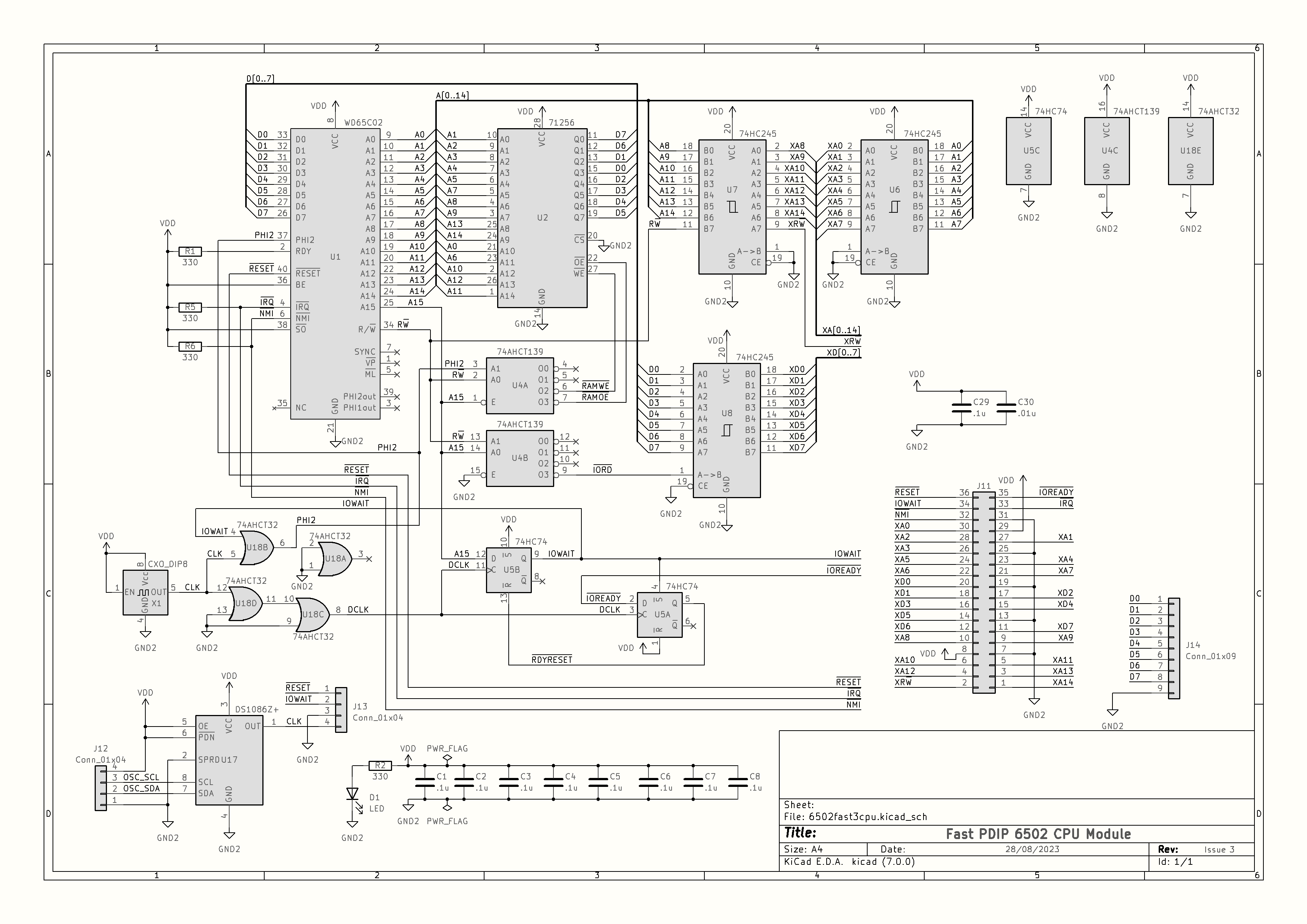
I thought I'd post an update. The breadboard prototype is stable at 25.175MHz again, with 64K RAM and the 16V8 PLD performing the decoding to decide whether to stretch the clock or not. This was rather hairy as I discussed a bit before. One big constraint has been the rise time for the high address lines of the CPU - on the breadboard I've seen times as bad as 20ns, though I think all the chips concerned are TTL-compatible so don't need it to rise all the way. In any case this restricts the maximum clock speed - the addresses start to transition shortly after the CPU clock falls, and I need to know whether to stretch the clock before it falls again, with a margin to account for the response time of the OR gate that's feeding the clock signal to the CPU. Adding the numbers up, this didn't sound too bad, but it wasn't working because my clock stretch circuit wasn't very well designed - it was originally meant to be a RDY control circuit until I repurposed it, and I think it suffers a bit from that.

There are really two things the circuit needs to know - it needs to know when an I/O operation is starting (so it can set a flipflop to stretch the clock) and it needs to know when the operation is complete (so it can reset the flipflop). The first one needs to get done somewhat before the clock would normally fall; the second one is less sensitive, but needs to happen at some point while the unstretched clock (CLK) would be high, so that when it resets the flipflop the CPU clock doesn't immediately respond with a short low pulse. In theory this could just be triggered by CLK being high, though in practice it seems to need a slight delay.

What I've ended up with is this:

Attachment:
schematic-64kpld-2023-09-10.png
schematic-64kpld-2023-09-10.png [ 36.54 KiB | Viewed 18039 times ]


No, I'm not very happy with it! It does work though, passing my RAM soak test and the Dormann tests consistently. I also tried applying heat to see if that destabilised things, using a hairdryer focused on the CPU, RAM, and PLD - it seemed fine though, at maybe 40C-45C according to my thermometer. The ICs were too hot for me to touch.

The changes here are that the OR gates are now HCT rather than AHCT, and there's an AHCT inverter that's taken over the A15 inversion (as it's a bit faster than the PLD was for that) and added some extra delays to DCLK2 and DPHI2, which push them towards the falling edge of PHI2. In theory I don't think DCLK2 needs all these delays, it could be driven straight from DCLK, but this is the configuration I stress-tested.

So I am happy that the 64K version is working, but I'm not sure if I want to commit this particular nonsense to a PCB - at the very least I'll need to make these delays configurable with solder jumpers or something like that. It may be better to just take another pass at this bit of the circuit from scratch as I think there's a simpler way - perhaps starting the timing from DPHI2 which needs to rise a little before the falling edge of PHI2, so it may make sense for that delay to come from a gate - rather than chaining gates together to try to delay for nearly the duration of PHI2 being high.

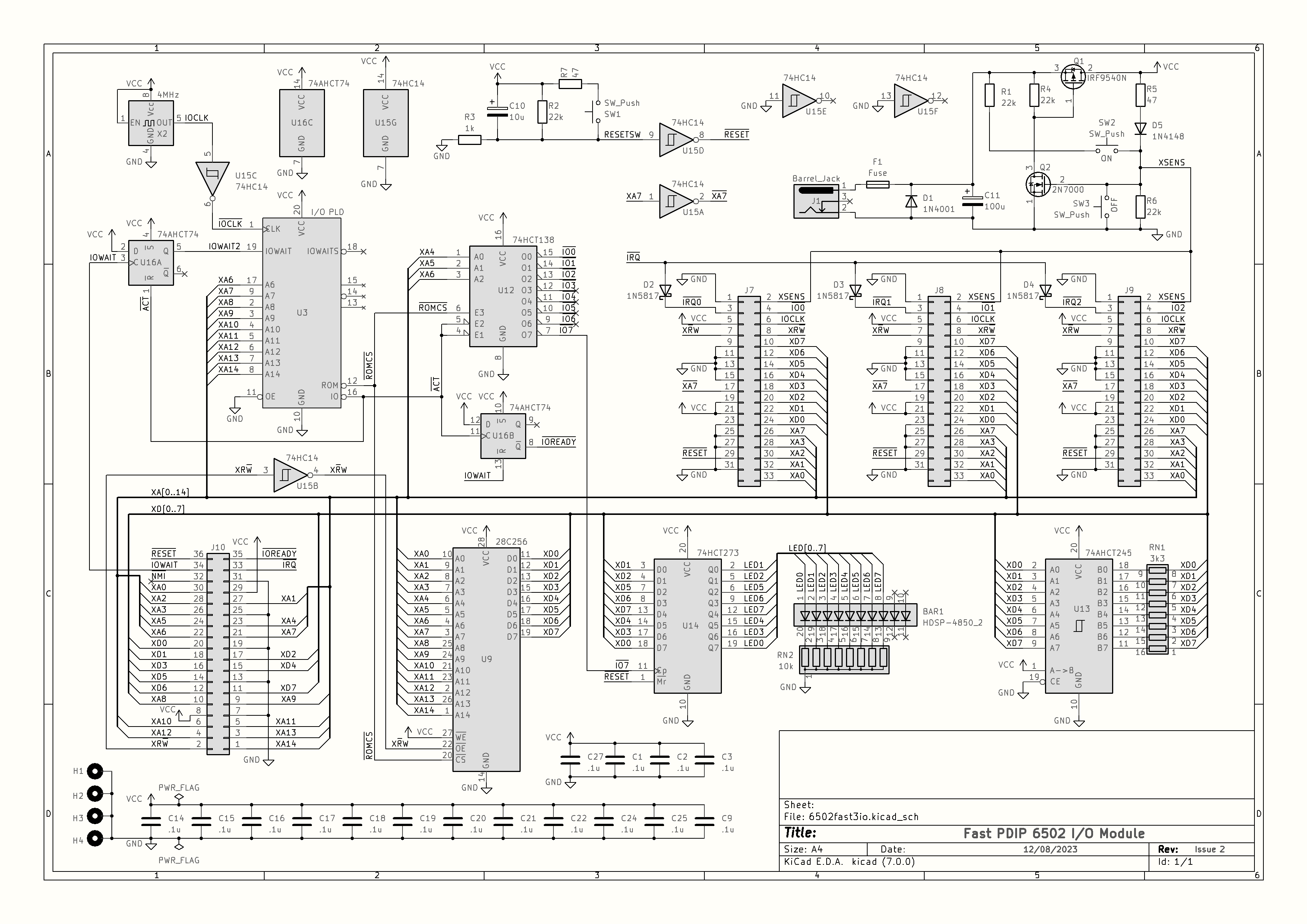
A related thing I've been working at is making it easier to connect the logic analyser to this circuit. Because of the clock stretching, and the high frequency, it is tricky getting it connected in a way that means it samples the bus at the right time and has its setup/hold times accounted for. To make this all much easier I built a circuit to go between the two, that latches the data bus and holds its value for the logic analyser to sample later on. This means the logic analyser needs to be triggered somewhat later than usual, and in turn this means we also need to latch the clock-stretching signal (roughly equivalent to RDY) that the LA needs in order to know whether or not to ignore the current clock cycle. I probably ought to latch RESET as well, but that's only being used to prevent data capture during long resets, so not very important.

This is the circuit I've ended up with - again involving another long delay line of inverters:

Attachment:
schematic-logicanalyserhat-partial.png
schematic-logicanalyserhat-partial.png [ 21.76 KiB | Viewed 18039 times ]


CLK is my main circuit's CLK signal, which preceeds PHI2 by at least an OR gate delay. So here, five inverters after the fall of PHI2, the internal clock line rises and clocks the register and D flipflop. Then one more inverter later the clock signal to the logic analyser falls, after which it samples the signals.

This particular configuration is what it took to work with my PCB prototype, at about 34MHz. It is not connected to the CPU's main data bus - it's connected through a further bus transceiver (74AHCT245) and I think that's why some of the extra gate delay was required here.

Again it feels like this delay needs to be adjusted for different circumstances and clock speeds. I am thinking of making this into a HAT (hardware-attached-on-top) for the logic analyser, to make it convenient and easy to connect, and maybe using jumpers to control the delays. Perhaps adding the possibility of even longer delays as well.

I also designed and prototyped an SD card interface module. I've usually done this through a 6522 in the past, but it can operate more quickly and with simpler code if the hardware has more direct support for it.

Attachment:
20230910_144710.jpg
20230910_144710.jpg [ 4.57 MiB | Viewed 18038 times ]


This uses another ATF16V8 PLD (probably the B variant, 15ns) along with an input shift register (74HC595) and an output shift register (74HCT166). There's also a 74HCT139 decoder as I ran out of macrocells in the PLD and didn't want to swap it for a more power-hungry one. Like my TTL serial module, this provides a fairly standard CPU interface - one memory-mapped I/O port for reading or writing data, and a control port where writes enable/disable the SD card's chip select, and reads read a flag saying whether or not the module is ready to read/write another byte. It can also generate interrupts when it needs attention, but I've mostly used it with polling so far:

Code:
sd_waitbyte:
    ; wait for busy flag low
    bit SD_STAT
    bmi sd_waitbyte
    rts

sd_readbyte:
    jsr sd_waitbyte
    lda SD_DATA
    rts

sd_writebyte:
    jsr sd_waitbyte
    sta SD_DATA
    rts


For a PCB implementation of that I should probably put the card socket and level-shifters etc on my own board, rather than using an off-the-shelf 5V adaptor module.

I'm happy to find that I can bolt on things like this fairly ad-hoc without worrying about wiring quality and signal integrity, and without causing any stability issues for the rest of the system - it is very convenient and makes prototyping new things very simple. I will probably do my floppy disc interface next.

Finally, I've been considering how I want to add video output support - in particular, ways of doing it without it being constrained to the slow I/O bus. At the moment I'm hoping to make it work through a narrow command-driven interface using just a few write-only locations that are not in the I/O address space - maybe a in zero page, for a little extra speed, or maybe just somewhere else in the RAM address space. Possibly an entire page, so that the address bus can do some work too, but I'm keen to avoid wiring a lot of signals through. Because these ports are write-only, the CPU doesn't need to wait and synchronise on a response - it does need to wait long enough before sending the next byte, but can use that time to get the next byte ready.

I want to make this work asynchronously this time, so that the CPU and I/O clock speeds are not tied in any way to the video pixel clock. The cost of synchronizing access is kind of high though - with two D flipflops between the clock domains I think it will cost at least 2 cycles of the video system before it actually reads the data, by my current calculations, it will be equivalent to about 2MHz communication rate with the video board, which is lower than I wanted. However through the use of FIFOs (74HC40105) I believe I can improve this significantly, and then the CPU can queue up 16 bytes of data at a time before having to wait.

Edit - one more thing regarding heat stress testing - my PCB prototype runs at 34MHz using the DS1086Z programmable oscillator, but fails my memory test after a minute or so of hairdryer heat. At 32.768MHz using a standard oscillator it seems completely stable under hairdryer heat, for several minutes with a thermometer saying the air temperature was 50C. The heat was focused on the CPU module, blowing hot air across both sides of the board (the RAM and some glue logic are on the back).


Top
 Profile  
Reply with quote  
PostPosted: Sun Sep 10, 2023 5:54 pm 
Offline

Joined: Fri Dec 21, 2018 1:05 am
Posts: 1076
Location: Albuquerque NM USA
I’m pleased to see you are getting to 34Mhz with DIP W65C02. My own experience with several prototypes and two pc boards also points to 33-36Mhz as max operation limit. Whether it is DIP or PLCC 6502 does not seem to have significant differences. I don’t think adjusting clock symmetry to have more time at high phase of clock matters much because we’ve already used the entire clock period from falling edge of clock to falling edge for logic decoding. We may get a bit more by tweaking the relationship of clocks to 6502 vs clock to decoding logic, but that’s tricky getting it reliable and producible over different parts manufacturers. Great update.
Bill

PS, another way to test the design margin is lowering supply voltage.


Top
 Profile  
Reply with quote  
PostPosted: Wed Sep 13, 2023 2:11 am 
Offline

Joined: Fri Jul 09, 2021 10:12 pm
Posts: 741
Thanks Bill

Today the PCBs I ordered a few weeks ago arrived - I did these on the cheap so it took a while. They were an updated CPU module with the edge connector the right way around, and a serial I/O card. So the system looks more like it was intended to now:

Attachment:
20230913_024145.jpg
20230913_024145.jpg [ 5.28 MiB | Viewed 17965 times ]


The board on the left is the new serial board, and the one in the middle is a VIA board with one VIA on it. I'm using this for timing things at the moment - I made it measure the CPU speed as I keep forgetting which oscillator I have installed:

Attachment:
20230913_024402.jpg
20230913_024402.jpg [ 2.36 MiB | Viewed 17965 times ]


In this case I have the programmable oscillator installed, and can change its frequency on the fly using an Arduino, which was interesting for testing. Memory tests still fail above 34MHz - there's no significant change to the core circuit here. Above 36MHz I start to also see random NMIs, although it is tied high - so perhaps there's some timing constraint on that within the CPU.

The serial I/O board is also working well, and much tidier than having a breadboard hanging off! The I/O slots on the motherboard are too close together, so when I rework that board I will spread them out more.

Here's the CPU speed measurement program. This works because the VIA clock is constant regardless of the CPU clock, so that can be used to time a specific period, and we can see how much work the CPU got done in that period. To do something like this in a system where the VIA clock is related to the CPU clock I guess you'd need some other consistent timing source, like a vsync, and have the VIA count those. The maths to calculate the value to display would be a lot more complex though - here I can choose the time period so that I don't need to do any maths at all!

Code:
measurecpuspeed:
.(
    php : sei

    ; Disable VIA interrupts
    lda #$7f : STA VIA_IER : sta VIA_IFR

    ; Wait for serial system to be idle
waitserialidle:
    bit SER_STAT
    bpl waitserialidle

    ; Clear pending serial interrupt
    stz SER_STAT

    ; We'll see how many times the CPU can increment a 2-byte BCD number within a certain period of time.
    ;
    ; The loop takes 21 cycles to execute.  If we timed for 21ms, the number we get would be the CPU frequency
    ; in kHz.  But we can't time for 21ms, as it's outside the range of a VIA timer at 8MHz.  So instead we'll
    ; divide everything by 10, and time for 2.1ms, then the high byte of the resulting count will be the number
    ; of MHz and the low byte will be the next two numbers after the decimal point.
    ;
    ; At 8 MHz I/O clock, 2.1ms is 2.1*8000 = 16800 VIA cycles, and we need to program the VIA with a value
    ; that's 2 lower in order for it to time accurately.
    ;
    ; We can then run our counting loop indefinitely, and let the VIA interrupt end the loop.

    ; CPU speed counter is stored in X:Y.  The code tends to slightly overcount, so round down by reducing the
    ; starting value by one (with BCD wrapping) plus another one for the carry that this causes
    ldx #$98
    ldy #$99

    ; We want to count in BCD, and start with the carry clear
    sed : clc

    ; Set T1 into one-shot mode, and set a high initial count so that it doesn't trigger before we're ready
    lda #$40 : sta VIA_ACR
    lda #$ff : sta VIA_T1CL : sta VIA_T1CH

    ; Enable T1 interrupt
    lda #$c0 : sta VIA_IER

    ; Set the IRQ vector to point to our code
    lda irqentry+1 : pha
    lda irqentry+2 : pha
    lda #<workloopend : sta irqentry+1
    lda #>workloopend : sta irqentry+2

    jmp pagealign

padding:
paddinglo = <padding
    .dsb 256-paddinglo,$ea
#print *-padding

pagealign:
#print pagealign

    ; Reset T1 to the value we want - 16800 ticks (8MHz * 2.1ms) minus 2 for VIA timer latency
    TIMERVAL = 16800-2
    lda #<TIMERVAL : sta VIA_T1CL
    lda #>TIMERVAL : sta VIA_T1CH

workloop:
    ; Update count
    txa : adc #1 : tax        ; 7 cycles
    tya : adc #0 : tay        ; 7 cycles

    ; Consider an interrupt
    cli : sei                 ; 4 cycles

    bra workloop              ; 3 cycles

    ; IRQ handler for exiting workloop
workloopend:
    cld

    ; Remove the interrupt frame from the stack
    pla : pla : pla

    ; Restore the original IRQ handler
    pla : sta irqentry+2
    pla : sta irqentry+1
    ; Disable the VIA interrupts again
    lda #$7f : sta VIA_IER : sta VIA_IFR

    ; Restore interrupt disable state and return with result still in X and Y
    plp : rts
.)

printcpuspeed:
    ; Push the count, low byte first
    phx : phy

    jsr printimm
    .byte "CPU speed: ", 0

    pla : jsr printhex
    lda #'.' : jsr printchar
    pla : jsr printhex

    jsr printimm
    .byte " MHz", 0

    rts


Top
 Profile  
Reply with quote  
PostPosted: Wed Sep 13, 2023 4:41 am 
Offline

Joined: Fri Dec 21, 2018 1:05 am
Posts: 1076
Location: Albuquerque NM USA
It is great to have programmable oscillator and able to measure clock automatically. You should be able to run faster with higher voltage, 5.5V is the absolute maximum. Voltage affects everything globally but localized heating of parts may find the weak link in the system. TTL speeds up when hot but CMOS slows down when hot so by selectively heating parts, you may find the speed bottleneck.
Bill


Top
 Profile  
Reply with quote  
PostPosted: Sun Sep 24, 2023 5:06 pm 
Offline

Joined: Fri Jul 09, 2021 10:12 pm
Posts: 741
plasmo wrote:
It is great to have programmable oscillator and able to measure clock automatically. You should be able to run faster with higher voltage, 5.5V is the absolute maximum. Voltage affects everything globally but localized heating of parts may find the weak link in the system. TTL speeds up when hot but CMOS slows down when hot so by selectively heating parts, you may find the speed bottleneck.

Thanks for suggesting this again - recently I got quite distracted by other things, but today I connected the PCB version to a variable power supply to try increasing the voltage. One thing I found was that with the supply set to 5V, losses in the cables, in my soft power circuit, etc led to the voltage around the CPU only being 4.6V. At that level it was stable at 34MHz, drawing about 0.4A. I increased the power supply voltage by 0.8V, and the voltage on the CPU board is now a little over 5.4V, drawing 0.49A. Set up like this, my memory soak test passes consistently at 38MHz, but the Dormann tests fail quickly at that level. They also fail at 37.5MHz, but pass consistently at 37MHz.

(My CPU speed reporting code says it's actually 36.66MHz, not 37MHz - possibly due to the "spread" feature of the variable oscillator, which I miswired in the PCB so it's always enabled. So it's likely that all these speeds I'm quoting are about 0.3MHz higher than the actual clock speed was.)

This is all with the original clock stretching circuit, not the new one I prototyped on the breadboard, and I think the original has some bad choices that constrain the timing unnecessarily. I need to find a bit of time to properly think it through though and decide whether I can test fixes for those issues on the existing PCB.

It is interesting to see the difference this voltage increase makes. I'm not keen to overvolt as a matter of course, but it's also shown that my circuit was actually undervolting before now. So in any new version of the PCB, I think I will add an on-board 5V regulator to ensure the voltage is consistent at that level regardless of power supply quality, losses in my soft power circuit, etc.


Top
 Profile  
Reply with quote  
PostPosted: Tue Oct 17, 2023 7:17 pm 
Offline

Joined: Fri Jul 09, 2021 10:12 pm
Posts: 741
I haven't got around to making any more progress yet on the hardware side with this system, but I've made some effort to publish some more information about it:


Also some of the demos extracted out into standalone repositories:

I don't think I actually shared the PCB layout here, so here it is in image form in case it's interesting, or in case you have suggestions for improvement - of course the KiCad sources in github are a better way to explore it than images, but here images are easier to post. These should match the schematics I've posted previously so I won't post them again redundantly, but will link to them here instead for your reference.

CPU module issue 3 schematic
Attachment:
File comment: CPU module issue 3 PCB design
6502fast3cpu-iss3-pcb.png
6502fast3cpu-iss3-pcb.png [ 470.37 KiB | Viewed 17719 times ]

I/O module issue 2 schematic
Attachment:
File comment: I/O module issue 2 PCB design
6502fast3io-iss2-pcb.png
6502fast3io-iss2-pcb.png [ 777.79 KiB | Viewed 17719 times ]


I'm not actually sure of the best way to capture this from KiCad, this is hand-composited in Gimp from exports of the top and bottom sides of the board - if anyone has better suggestions for how to do that and get a clear result then please let me know. And apologies to the colourblind - I wasn't sure of a good way to export this kind of thing without relying on colours.


Top
 Profile  
Reply with quote  
Display posts from previous:  Sort by  
Post new topic Reply to topic  [ 111 posts ]  Go to page Previous  1 ... 4, 5, 6, 7, 8  Next

All times are UTC


Who is online

Users browsing this forum: Google [Bot] and 8 guests


You cannot post new topics in this forum
You cannot reply to topics in this forum
You cannot edit your posts in this forum
You cannot delete your posts in this forum
You cannot post attachments in this forum

Search for:
Jump to:  
cron